This thread has been locked.

If you have a related question, please click the "Ask a related question" button in the top right corner. The newly created question will be automatically linked to this question.

Noise Measurements with ADS1259EVM and PGA280

Other Parts Discussed in Thread: PGA280, ADS1259, ADCPRO

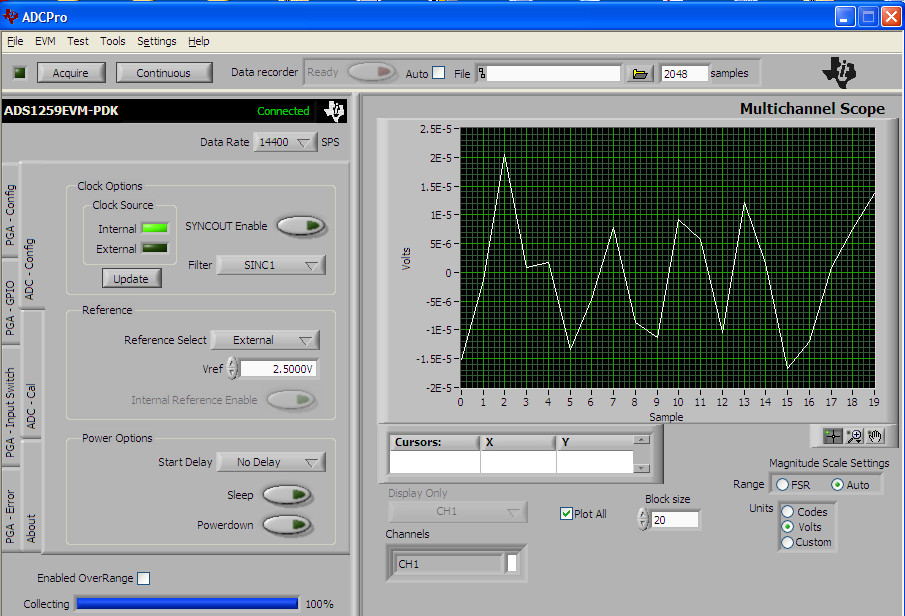
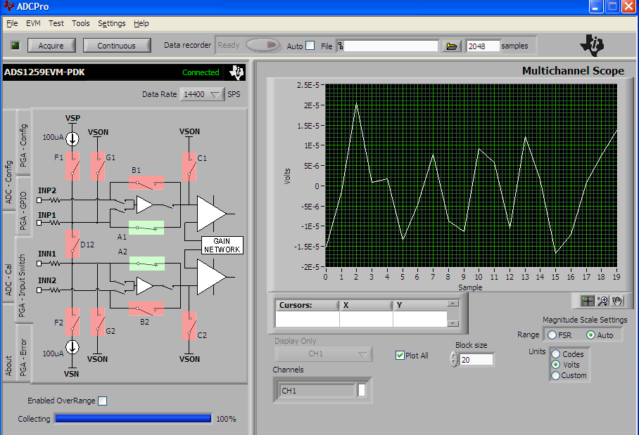
I try to evaluate the ADS1259 using an ADS1259EVM development board. 

I need to do some noise measurement with both inputs of the PGA280 of that board to ground. I use external reference (the one on the board) and the VOCM is connected to half AVDD.
When I do measurements at 60SPS with SYNC2 enabled I read values close to 0V from ADC. However if I change to 14Ksps and disable SYNC2 (with the same setup - analog input of the PGA280 connected to ground) I read from ADC values around -2.49V.
What could be the issue?
  • Hi Gary,

    You should be able to obtain readings close to zero in both data rate/SYNC filter condigurations; I suspect a setting or the voltage supplies are not configured correctly. Can you please confirm the settings of the following:

    - MMB0 supplies: The ADS1259-PGA280EVM requires +/-10V (up to +/-15V) external voltage supplies connected to the MMB0 Motherboard.  This voltage supply could be fed through J14 +/-VA on the MMB0.  The bipolar analog supply feeds the input stage VSP/VSN voltage supply of the PGA280.  This voltage can be also verified at J11.1 and J11.2 of the ADS1259EVM board. Is this voltage supply on?

    - Switch S2: Middle Position (ADC Inputs to PGA outputs); Switch S3: Middle Position (AVDD/2); Switch S1: Right Position (REF5025 On Board Reference)

    - INN1 (J8.3) and - INP1 (J8.4) Shorted together and Connected to AGND.

    The ADS1259 is set up at 14400SPS (with either SYNC1 or SYNC2 filter).  The PGA is set up with Gain 1V/V.  Please see the settings on the PGA Input Switch and ADC Configuration tabs below:

    Best Regards,

    Luis


  • Hi Luis,
    Below is my customer's response to your suggestions, it seems he is still seeing the problem persist.  Can you make some other recommendations?
    - Yes, +/- 12V are present at J11.1 and J11.2 on the ADS1259EVM
    - Yes, Switch S2 is in the middle position (ADC inout connected to the PGA output)
    - J8.3 and J8.4 are individually connected to AGND (J8.9 and J8.11)
    - The ADC is setup at 14400SPS (with SYNC1) and PGA gain is 1V/V (please see the PGA, ADC registers bellow)
    PGA registers
    0x00 0x18
    0x01 0x00
    0x02 0x20
    0x03 0x19
    0x04 0x00
    0x05 0x18
    0x06 0x60
    0x07 0x00
    0x08 0x38
    0x09 0x20
    0x0a 0x00
    0x0b 0x10
    0x0c 0x00
    ADC registers
    0x00 0x25
    0x01 0x08
    0x02 0x57
    0x03 0x00
    0x04 0x00
    0x05 0x00
    0x06 0x00
    0x07 0x00
    0x08 0x40
    Another thing: if I read continuously from the ADC using above register values (and the PGA inputs to ground) I get values around -2.49V. Once I switch S2 to calibration position (without re-initializing anything is software) the values read are close to zero.
    The voltages measured on both TP7 and TP8 are around 2.5V when S2 connects the PGA to ADC input.
  • Hi Gary,

    The PGA280 register settings above appear to be correct; the PGA280 is set at a Gain of 1 with SWA1 and SWA2 closed  (connected to J8.3 and J8.4 header inputs).
    The ADS1259 is set up to be used with the external Reference, SINC1 Filter, external CLK, Pulse control mode at 14400 SPS. 

    When the VOCM pin on the PGA280 is connected to half AVDD; and the inputs of the ADS1259 are connected to the output of the PGA280, the voltage at TP7 (AINN), TP8 (AINP), TP12 (VON) and TP11 (VOP) should be around +2.5V; as described above. 

    A few more questions:

    - Switch S1 should be in the Right Position (REF5025 On Board Reference); Is this correct?

    - If the customer applies a voltage, i.e. +1V, to J8.4 (INP) and GND to J8.3 (INN) does the customer obtain the expected conversion?  What are the conversion results obtained in codes? What are the voltages across TP12 and TP11?

    - What are the conversion results in codes when the J8.4 and J8.3 are shorted and connected to AGND?

    - -- Just to clarify, it appears the customer is using the ADS1259EVM stand alone using their own software (without the MMB0 motherboard). Is this correct?  Does the customer have the MMB0 board available? If this assumption is correct, can the customer repeat the same experiments using the ADS1259EVM+MMB0, with the ADCPro plugin, to verify that the hardware works as expected?

    Best Regards,

    Luis