This thread has been locked.

If you have a related question, please click the "Ask a related question" button in the top right corner. The newly created question will be automatically linked to this question.

Questions about TLV5637 Digital Analog Converter

Other Parts Discussed in Thread: TLV5637

Hello everyone!

I have a few questions about the TLV5637 DAC. I'm using the MCP2210 USB to SPI chip to control the SPI data sent to the DAC.

I know how to sent the data. The problem is that I'm not sure if I'm sending the right data. In the datasheet of the chip I says that first 4 bits of the 16 bit word to send are the control bits. I set them up to select DAC A output and external reference voltage (0xD003 - '1101 0000 0000 0011). I then send this via the SPI interface to the DAC.

Right after I do this first transfer I set up the next 16 bits. I have a trackbar that goes from 0-1023 (0x00 to 0x3FF - max 10bits). The first 4 bits are again set up for updating the DAC a output (0xC000). I add to these bits the value of the trackbar*0x0004 to keep the final bits as reference.

This is my conundrum. Do I have to actually send a 12 bit code (disregarding the final 2 bits) or a 10 code for the DAC value? As long as I set up the reference in the first flow of bits do I need to set it again the second one?

I've been trying to figure out this for a few days now.

I hope I was clear in what my problem is.

Best regards,

Robert Iagar - SC Continental Automotive Romania SRL

  • Hi Robert!

    Welcome to our forum! 

    For the TLV5637, when you write to the control register (R1=R0=1) you don't actually write anything to the data buffer - you are only configuring the reference.  You only need to do this once after power up.  With D1=D0=1 you are selecting the external reference option as noted above, so the first access would be 0x9003.  To output a ramp, you should be able to write 0xC000 through 0xCFFC (your 0x3FF left shifted to MSB align the data).

  • So the values are always between 0x000 and 0x3FF, but each time I left shift 2 bits. 

    Also every time I need to keep D1=D0=0?

    The only thing I don't understand is how do I calculate the output voltage to display in my application? In the datasheet it says that the code goes through 0x000 to 0xFFF which is a 12 bits max, but the DAC only supports 10 bits. I am missing something? Do I have shift them also?

    Really confused. Your previous answer helped. Will try to implement something tomorrow.

    Thank you for your prompt response.

    Best regards,

    Robert Iagar - SC Continental Automotive Romania SRL

  • Hi Robert,

    Yes, that's right; left shift by two.  There is a formula on page 10 for the output voltage versus code input.  There is an inherent gain of two followed by CODE/0x1000.  Code 0 then gives you 2*Vref*0/4096 or 0V out.  Code 3FF, left shifted by 2 is FFC so with a 2.048V reference, you have 2*2.048*4092/4096 or 4.092V out.  D0 and D1 do not have to be '0' - they are simply ignored by the DAC.

  • Today I will try and use the left shifted code as the CODE in the formula. Sorry for the late reply. Thank you for all your help. If I have further questions or issues I will not hesitate to ask :)

    Best regards,

    Robert Iagar - SC Continental Automotive Romania SRL
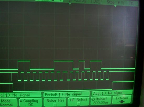
  • Here's a osciloscope graph of the data I send through the USB to SPI application that I built. The reference is set to external and it 3.3 (3.256 measured with the Voltmeter). The code sent is C3AC and the output of the DAC is 1.034 V, but the calculated voltage with the formula is 1.4945 V.

    Where am I doing things wrong? This is becomming a litte bit frustrating. Hope it's not transferable.

    Thank you very much for your support.

    Bottom trace is the nCS, middle one is the CLK and the top one is Data.

    Best regards,

    Robert Iagar - SC Continental Automative Romania SRL

  • Hi Robert,

    Thanks for the screen shot!  Take a look at note (1) on the bottom of page 3 of the TLV5637 data sheet and let us know what your VDD rail voltage is.

  • The REF and VDD pin are connected to the same line which is 3.245 (3.3) V.

    This is the problem right?

  • Quite possibly - can you add a resistor divider to the VREF pin or perhaps source it differently by lifting the pin and see if that resolves your problem?

  • Unfortunately I can't. The chip is already soldered to the board. I didn't build it. I just make the software for it. I'll see what can I do.

    Thank you for your continued support. I guess that my software is okay, the way the board is built is the problem.

    Again, thank you,

    Robert Iagar - SC Continental Automotive Romania SRL