This thread has been locked.

If you have a related question, please click the "Ask a related question" button in the top right corner. The newly created question will be automatically linked to this question.

ads1211 circuit recommendations

Other Parts Discussed in Thread: ADS1211, OPA365, ADS1256, ADS1278, ADS1294, ADS131E04, MSP430G2211, ADS1298

Hello everyone, I am doing a small project in university and need to acquire data from three industrial single ended transducers. I need at least 16 bit, 2000 SPS sampling.

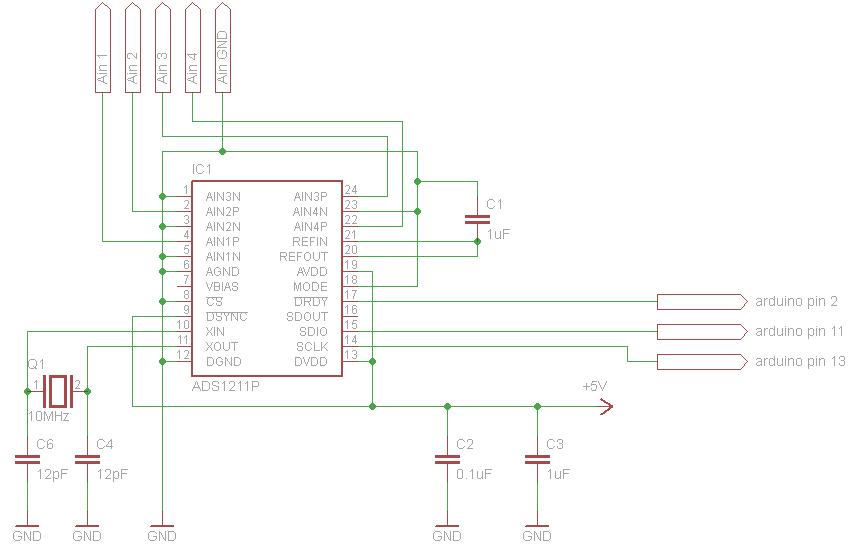
I chose ADS1211 adc chip, as there is a fully working library for arduino microcontroller.

I have it working, but it has a significant amount of noise. I read the Design Notes section about ground of the circuit, which I found very useful.

I have a few questions regarding noise reduction as follows:

1. I power adc circuit from the arduino 5 volt output. Would a separate power source for the adc circuit reduce noise?

2. Would an external low noise, low drift voltage reference as REF5025 help? Also if I am using the REF5025, should I use the buffer circuit with OPA365 as recommended in ADS1256 datasheet, figure 26, p. 29.

3. There is a recommended circuit for data acquisition in REF5025 datasheet (figure 34, p.12) with OPA365 op amp for the signal input. Does OPA365 circuit improve the results? And is there a cheaper and more manageable alternative to OPA365 (the chip is so tiny, I have no idea how the hobbyist would be able to use it).

4. Finally, is digital isolator unnecessary for the SPI interface, to isolate microcontroller noise from the adc circuit?

Any recommendations and comments are welcome.


  • Vilius,

    Welcome to the forum!  You should make sure that your power supply to the ADS1211 is clean, and that your supply inputs to the ADS1211 are bypassed with caps.  You can check to see how noisy the Arduino supply is with an oscilloscope. 

    You should be able to achieve good performance with the internal reference of the ADS1211, but you should have a cap at the input at the REFIN pin.

    You do not need digital isolation.  You could add some small series resistors (33 to 50 ohm) to slow down edges of the digital signals.  A bigger concern is layout.  You must make sure no digital signals interfere with analog signals.

    Can you send us your device settings?  How much noise are you seeing?  Can you send us your schematic and layout?  We are willing to take a look and suggest improvements as needed.

    Best regards,

    Bob B

  • Hello Bob,

    thank you for the reply and reminder about bypass capacitors. Completely forgot about them and they made a big difference.

    I am using a general schematic from the datasheet figure 12, p. 18. I soldered everything onto arduino protoshield and do not have the pcb layout at the moment, because I want to find the best chip for my needs.

    I attached the schematic, I am currently using. All AinN pins are grounded, because all transducers output 0-5 V and 99 percent of the working range is in 1-4 V region.

    Also I use one point to ground all the grounds, to avoid voltage difference.


    At the moment, if I read one-two channels at 2000SPS with PGA 1, TM 16, DR 194 and 4MHz clock I get only 0.5 mV ripple, which is a very good result, and what I aim for!

    BUT if I switch between all three-four channels, the noise increases to 5mV. I tried low pass RC filter for the inputs, without any noticeable results. Maybe I chose the cut off 1000 Hz frequency too high?

    What's more, there are two more strange things happening.

    Firstly, the voltage output increase/decrease at one transducer influences other channels readings for some reason(when I read all four channels). EDIT: I think I answered this question myself. When I reduce the clock speed and DR, Channel readings become stable. It looks like I want too much from the chip.

    Secondly, if I use turbo mode 1-8, the input cuts of around 200-300 mV and show a lower value. I get the same voltage value as multimeter only at turbo mode 16.

    What could cause that?

    My main concern at the moment is the data conversion time, for each channel. With turbo mode 16 and clock cranked up to 6 Mhz, it takes around 2ms for each channel to read data, which is quite noisy. To achieve satisfactory results it takes anything up to 15-20ms. I have only 150-180ms time window, where I need to take 300  samples from three transducers. Those samples must be acquired with as little time delay as possible.  Maybe I should learn to solder smd components and look for simultaneous adc chips? Any recommendations? ADS1278, ADS1294, ADS131E04 caught my eye in your catalogue. 

    I am studying mechanical engineering, and just try to expand my knowledge to electronics during the summer. The learning slope is high, but I am not giving up, even though the sun is shinning outside :)

    Any recommendations of references to information is very welcome.

    Looking forward to the answer.

    Best regards,

    Vilius 

  • Vilius,

    I am impressed that you chose to learn something new...but you should also enjoy your summer. :)  There are many relationships in the work place where mechanical and electrical engineering work for a common goal.  You are wise to familiarize yourself with the electrical.

    You are most likely seeing two issues.  This first is noise as it relates to layout.  To get high levels of performance, you must make sure that your all your traces (wires) are clean and that the digital signals do not in any way interfere with analog.  Grounding is often overlooked, or misunderstood as you must think of the total current path (which also includes the return path of signals.)

    The second issue is digital filter settling.  Any time you switch signals through the mux you have a step response.  It takes time for this voltage to settle both in the analog domain and the digital domain.  The term latency is used to describe the time it takes for the digital filter to settle.  At the slower data rates, or if you do not switch the mux as often, you will not notice the degree of the filter settling.  In the case of the slower data rates, the digital filter has a higher decimation and basically averages out the value obtained (which also averages out the noise to improve that issue as well.)

    To try a differenent device, it might be helpful for me to know your target resolution.  I think I understand your timing requirements and input voltage range.

    Best regards,

    Bob B


  • please i need to use SPI  Msp430g2211  with ads1298   please help me

    i need exmaple for spi please