This thread has been locked.

If you have a related question, please click the "Ask a related question" button in the top right corner. The newly created question will be automatically linked to this question.

Noise analysis, ADS1247, 4-wire mode with RTD

Other Parts Discussed in Thread: ADS1247, ADCPRO

Hello:

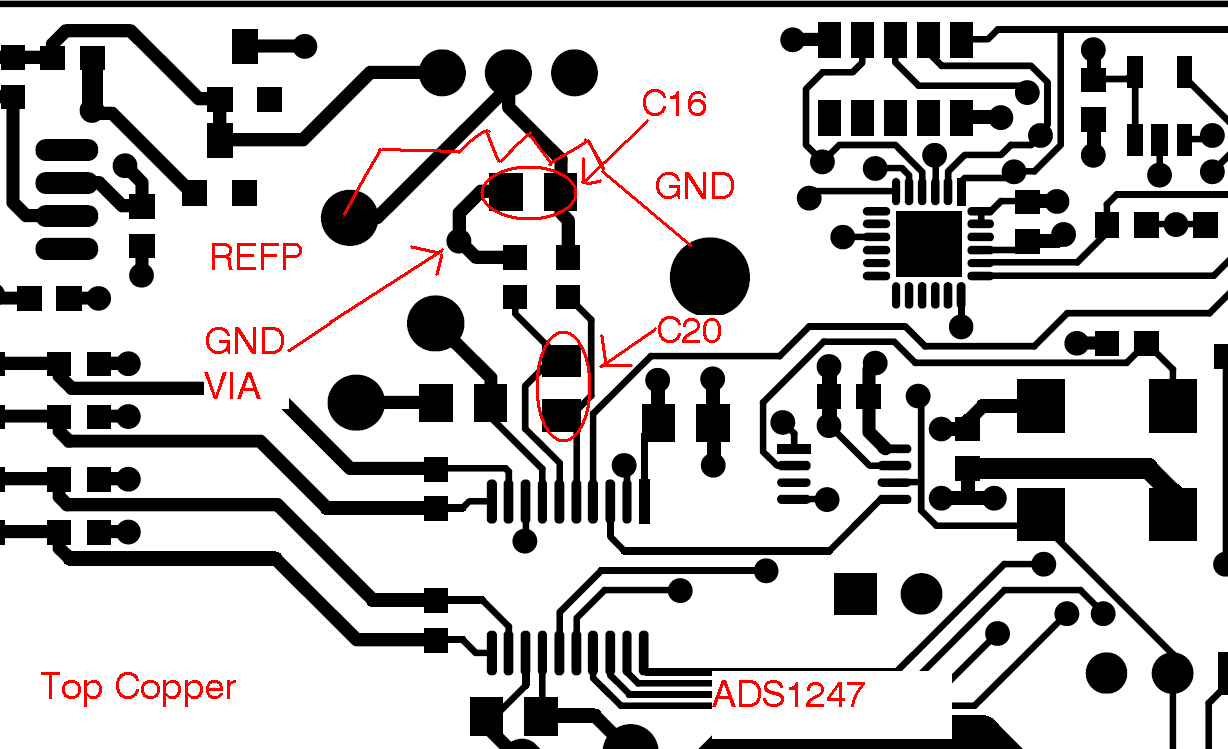
I've been successfully evaluating an ADS1247 with the EVM and EVM-PDK eval boards. I was happily surprised that this setup -- being powered via USB -- is giving me noise numbers nearly exactly the same as the spec sheet. This is with the inputs (AIN1 and AIN2 shorted). Other important setup data:

Rbias = 2.5k

IDAC = 1mA (sourced through AIN0)

Sample rate 5, 10 and 20 SPS.

PGA gains of 4 and 8

However, when I un-short the inputs and measure resistance across my RTD my noise goes up considerably maybe by a factor of 10. I am used four 100ohm RTD in series so nominal resistance of my composite RTD is 400 ohm.

I've had long experience developing low noise front-ends and typically the first pass has noise way greater than expected so I am not discouraged but I do need to get some ideas as to how to optimize noise performance.

So my question to you is: Are there noise sources in the ADS1247 that do not show up with the inputs shorted but are seen when the circuit is configured reading an RTD?  For instance, the IDAC source would have non-zero noise that would show up as a time varying  voltage across the RTD. At first blush I would say that the IDAC noise will get cancelled out by the fact that I am running the IDAC current through my 2.5k Rbias resistor that is setting Vref. However, if there were some sort of time delay between the noise on the IDAC source and the time that the ADC sees a change in voltage (due to the IDAC noise) then the noise would not have perfect cancellation.

Then there is the thermal (or 4kT) noise generated by the RTD and by the Rbias resistor. These would be non-corrolated sources that would show up as noise. But my calculations suggest that due to the fact that my sample rate is so low, (meaning my measured input bandwidth is very low) the thermal noise from the RTD and Rbias would be insignificant.

The other noise source that could muck up the works could come from 60 Hz. I've tried hard to shield my system in a grounded enclosure and also the ADS1247 does 50-60 Hz filtering on the sample rates I am using. Additionally, when I look at the 'scope traces' or FFT outputs through the NI interface I cannot detect significant line frequency noise.

So, with all that said, can you give me more insight as to where noise might be being generated and measured in my setup such that I would see noise quite a bit bigger than spec'd inthe spec sheet?

Thank you for your time on this matter, the ADS1247 seems like an awesome device and we have many uses for this part if I can tame the noise.

Rich

  • Rich,

    There are a couple of things that are not clear.  Do you have your RTDs connected to the EVM?  Are you using 2 wire RTDs?  Can you send us a schematic of how you are connecting things up, as I can't visualize how you are doing this?  Can you send us some data?  This can either be raw data or pictures from ADCPro if that is what you are using for analysis.

    Noise is a problem with any system.  In particular, the noise performance tables you mentioned in the datasheet are best case scenarios with shorted inputs.  In practice it is really hard to match this in a system.  From your discussion it appears you have a good understanding of the noise problem.    Layout is a huge concern in overall performance.  Also, I would gain to the maximum possible gain staying within the common mode input range.  The actual noise becomes less dominant with gain.  This seems counter intuitive, but the signal to noise ratio does increase.

    If you are using the EVM, there are a couple of things to consider.  The first is the Rbias resistor should be placed close to the reference inputs.  The EVM doesn't really allow you to do that easily.  As you mentioned, noise should cancel in a ratiometric system.  However, any filtering will affect the phase difference between any filtered input and filtered reference.  The EVM has a 10uF cap near the reference inputs, and analog inputs also have filtering.  The analog filtering also effect the current path.  Another problem that can add noise with the EVM is the protection diodes (D1 and D3) at the external reference inputs.

    Another thing to consider is aliasing, and any high frequency signals (EMI/RFI) that can noise up your readings.  To eliminate this issue you need a low pass filter at the input.  If you are using a two wire RTD, any filtering done within the current path will affect the result.  With a three wire RTD you can have two current paths and cancel the series voltage drops.  If you are making a single measurement across all four RTDs at once, which is what I think you are doing, I would remove all components relative to AIN0 (R4, C7 and C24) and actually make the measurement across AIN2 and AIN3.

    Best regards,

    Bob B

  • Hi Bob:

    Thank you for your detailed response. I will try to answer your questions.

    I am measuring the temperature of a block of copper that is about 50mm square and about 6mm thick. I am using four 2-wire RTDs that are embedded in the copper. The leads of each RTD protrude from the block and are soldered to pads on a PCB that is mounted to the copper block. The traces on the circuit board then connect the four RTDs in series. At the 'top' and 'bottom' of the RTD 'pole' I have two traces meeting at the RTD lead. This constitutes my Kelvin connection ( I realize that there is still some lead resistace error in the traces that connect one RTD to the next). The four PCB traces (+/- Force and +/- Sense) route to a connector. Then through a connector the four wires are brought to the EVM. The + Force wire is connected to screw terminal AIN0, + Sense is connected to AIN1, -Sense is connected to AIN2. The -Force wire is connected to header J8 pin 20 (Ref+). My 2.5 kohm 5 ppm resistor is soldered between pins 20 and 18 of J8 (Ref+ to Ref -).  As you said this places the Rbias resistor more than an inch from the ADS1247 chip.

    So my circuit looks near identical to the Figure 4 of apps note SBAA180 (Four wire RTD Example) except that I am using AIN1 as the (+) sense and AIN2 as the (-) sense. Is that a problem?

    I have attached a screen shot from ADCPro. Note PGA gain =4, Data Rate 5sps. The time scale is such that the complete sweep is 410 sec.

    For this measurement, my copper block had been in a highly insulated cylinder overnight. The input sensitivity of four 100 ohm RTDs in series (and IDAC = 1mA) is 1.54 mV/degC. The vertical scaling shown is 3 uV/box which translates to 1.95 mdegC/box. The range of the temperature window shown is 23.3 mdegC. With your eye you can remove the DC component and try to estimate RMS noise. When I do that I come up with a pkpk noise of about 5 boxes or 9.75 mdegC. Assuming gaussian noise that gives you an RMS noise of about 1.62 mdegC (divide pk-pk by 6).

    Converting my measurements to ADC counts (or LSBs): Because the PGA gain is 4, the full scale input to the ADC is not +/-2.5V it is +/- 2.5V / 4 = +/- 0.625V (RTI). So the value of an LSB is 1.25V / 2^24 = 74.5 nV.. As mentioned above, my vertical scaling is 3 uV / box. This translates to 3 uV / 74.5 nV = 40.2 LSBs per box.

    Also, from above, my noise is about 5 boxes pk-pk which is also then 5 x 40.2 = 201 LSB pk-pk or (again dividing by 6) = 33.5 LSBs rms.

    When I short the two inputs together under this gain and data rate I measure 5.27 LSBs rms (or 0.393 uV rms which matches the data sheet value of 0.37 uVrms)

    In summary, with shorted inputs I get noise of 5.27 LSB rms. When have the RTDs in the circuit I get noise of 33.5 LSB rms --- larger by a factor of 6.4.

    Looking closely at the EVM schematic I see now the problems that could be generated by the input filters to the ADC and especially the 10uF cap (C20) that is in parallel with my 2.5k Rbias resistor. By the way that the EVM is implemented where C7 goes across AIN0 and AIN1 while C8 goes between AIN2 and AIN3 it seems to suggest that voltage measurement should be taken across either AIN0/AIN1 or AIN2/AIN3. I'm measureing across AIN1 to AIN2 which seems not quite right for the filtering setup.

    Above you say to remove R4, C7 and C24 and measure across VIN2 and VIN3. Should I not also remove C8, C20 and D1 and D3 ?

    Thanks, Rich

  • Rich,

    I would remove all components relative to the AIN0 input (you will have to replace R4 with 0 ohms, or preferably a short across the terminals), then use AIN2 and AIN3 for your sense connections.  You will see the largest benefit from the differential cap, which you do not currently have in your setup.  So I would not remove C8.

    I would remove the diodes at the reference input as you are generating the reference from internal sources, you don't have to worry about overvoltage protection.

    Before removing C20, I would look to see if there was any reduction in noise with respect to the input filtering.  I would also compare the internal reference to the external reference.  If you do not see any improvement, or if the internal reference provides better results, then I would try to improve the reference circuit by any means possible.  If you are using a leaded Rbias resistor you could attach across the test points REFP and GND.  If using a SMD resistor, you could try soldering it on top of the C20 cap (or removing C20 and using the existing pads.) This assumes the SMD resistor will fit in that space.  Notice that C16 is also in parallel, so you may want to remove that device and/or use it as pads for Rbias.  If your resistor is SMD and larger than the existing pads, you may be able to fit in one of the two cap spaces by angling the resistor slightly and scraping off a little bit of the soldermask from the copper trace then soldering the resistor in place.  This extra effort should help by lowering any inductance associated with the reference path.

    Best regards,

    Bob B

  • Bob:

    Great ideas. Just the kind of insight I was hoping for. I now have a number of things to try.

    Especially easy will be to try the internal ref ( I think that requires switching the physical switch S1). As I understand it, I should see an increase in noise with the internal reference because I've lost the ratiometric advantage. And you are saying that there is no way that using the internal ref should be less noisy than using external ref.

    My Rbias resistor is a Vishay-type radial leaded part so that gives me a lot of options for placing on the board.

    I'll keep you posted.

    Rich

  • Hi Bob:

    A follow up from our last correspondence. I was able to make significant strides in lowering system noise. Many of your suggestions helped but one of the bigger helps I found on my own.

    For reference, when I first started this thread I was measuring an input referred noise of about 2.5 uVrms, now I am getting noise RTI of 1.05 uVrms. This is a big difference. (conditions: Vref = 2.000V, PGA = 4, sample rate 5sps) As you know from working with noise power, to decrease the measured rms noise by a factor of 2, you need to remove almost 87% of the original noise sources. [ sqrt(1^2 - 0.866^2)] = 1/2

    These are the changes I initially made to the EVM circuit and configuration:

    1. Changed the wiring of the sense leads so I use AIN2 and AIN3 as inputs
    2. Removed D1 and D2 (showed measureable difference)
    3. Moved my 2k Rbias resistor closer to the ADC as you outlined
    4. Removed C20, the 10 uF cap around Rbias.
    5. Removed and shorted R4, removed C24 and C7

    With the changes above, I still saw what seemed to be bursts of noise lasting 1 to 4 seconds that would mess up my readings. This looks a lot like popcorn-type noise.  To investigate this, I used a very low noise high gain scope pre-amp (Tek ADA400A) and measured directly across my RTD to look at the voltage that the ADC is seeing. What I found on the scope was this popcorn noise effect correlated exactly with what I was seeing in the EVM (LabView) interface.

    My reading of this is that the popcorn noise is coming from the IDAC source. I switched IDACs and saw the same noise. So what I did to significantly reduce this effect (although I can still see it) was to:

    1. Put a capacitor back into the location of C24, but instead of 47 pF I used the 10uF cap that I had removed from C20.

    This 10 uF capacitor, along with the series resistor values of R4 and my RTD (nominally 400 ohm) places a low pass filter on the IDAC at 35.6 Hz.

    So with the above changes, and the big filter on IDAC, I was able to reduce my input referred noise by a factor of 2.5.

    My temperature measuring system now has noise in the range of 700 uCrms (micro degrees C) and this is without averaging which could beat the noise down even further.

    Pretty awesome device... If the IC designers were able to reduce the popcorn noise on the IDACs it would be even more awesome.

    Rich