This thread has been locked.

If you have a related question, please click the "Ask a related question" button in the top right corner. The newly created question will be automatically linked to this question.

ads1282 noise problem

Other Parts Discussed in Thread: ADS1282

Dear Community

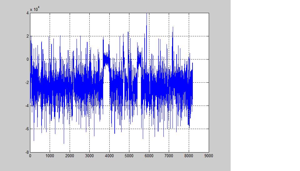
I currently used ads1282 adc in a project, according to the datasheet, the noise rms value should be around 1.1uV@1ksps  by snr=20log10(Srms/Nrms), however, the tested result was about 30uV, i am not sure if there was something i missed.

the following is the test environment:

dvdd=3.3V

avdd=2.5V,avss=-2.5V

vrefp=2.5V,vrefn=-2.5V

bypass pin connected to a 1uF capitor

mclk=4.096MHz

1ksps, gain=1, mux=3'b010 - use internal resistors connected to (avdd+avss)/2 to test noise rms value.

the above picture is the noise wave in time domain.

Thanks for any answer.

ingdxdy

  • Ingdxdy,

    Welcome to the forum!  One consideration is properly looking at the SNR specification as AC response versus DC response.  Due to optimization and filtering, the performance  will be less than expected for DC.  I'm not sure what kind of measurement you want to be taking, but generally you wouldn't use the ADS1282 for DC or very slow moving inputs without using additional post processing.  If you average a number of samples you can achieve a better noise level for DC measurements.

    If you will be using an AC input, then it is better to apply an AC signal and run a FFT to verify your SNR.

    Best regards,

    Bob B 

  • Hi Bob,

          i just want to check the noise floor as fig.7,8 shows in the datasheet.

    i shorted  diff input and read out the sampled data from spi interface, ploted the data in matlab and calculated the rms value - (norm(data)/sqrt(length(data)), and then converted to voltage by 5/2^31*rms.

    i did not do averaging of the data, i am not clear what it means that you say 'using additional post processing'.

    the plotted noise wave(show below) in time domain indicates there is something unstable in modulator or digital filter, my reference voltage is generated from adr445 , and avdd and avss are all generated from LDOs. 

    in fact, when i directly shorted capp and capn pins, the sampled noise was still large that was around 30uV, so i think the pga is not the reason.

    Regards,

    ingdxdy

  • Ingdxdy,

    Figures 6 and 7 are FFTs.  I'll run some histograms and post them as soon as I can.  Unless you apply 20mV DC between the inputs you will see a tone, and that may be what you are seeing in the graph.  I'll have to review your calculations to make sure I fully understand what you are doing and seeing.  30uV rms is excessive.  From my recollection it should be only a few uVs rms.

    The post processing I was referring to is primarily averaging.  Proper layout is critical for this device to meet performance levels.  Can you share your schematic and layout?

    Best regards,

    Bob B

  • Ingdxdy,

    My colleague has previously taken some data over various data rates and gains.  These measurements were taken using the ADS1282EVM with the inputs shorted and the common-mode voltage set by placing a voltage divider between VREFP and VREFN.  I've provided it below:

    Best regards,

    Bob B

  • Hi, Bob

         Thanks for your quick replying.

         According to the datasheet, the noise should be around 1.1uV@1ksps, but the tested result was about 30uV!

    After doing averaging(8), the noise does not change much and is still unacceptable.

    the schematic and layout show below.

    Regards,

    ingdxdy

  • Ingdxdy,

    As you can see from the data I sent, you are getting much more noise than you should be seeing.  I can't really tell from the layout where the reference is coming from.  Reference noise will effect the results.  I'm assuming that you have power and ground layers.  Is there any chance you can send me your raw data?

    Best regards,

    Bob B

  • Hi Bob,

         As you said, power and reference are provided by power planes, in fact, the reference output drives at the same time four 1282s, but in our test, we only soldered only one 1282. Does it influence much? should one reference drive only one adc directly? we used such driving method in past designs and it functioned well.

    you can find the raw sampled data in the attachment.

    the data has been processed using following formula.

    de=((h&0xff)<<24)|((m&0xff)<<16)|((l&0xff)<<8)|((f&0xfe));
    de=de/2;

    where h is the MSB-byte, f LSB-byte.

    Best Regards,

    ingdxdy

    2335.test1282.dat

  • Ingdxdy,

    I may not be interpreting and reading in the data correctly.  How many samples are in the data file, and are they signed 32 bit values?  I assumed the data was signed 32, and had a series of 8192 samples.  However, It appeared that the graph you placed on the forum is 1024 samples.  One thing I noticed when I imported the data is the samples repeated.  In other words every value appeared twice, so I'm assuming that maybe I imported the data incorrectly.

    An interesting thing is with the import I too got about 30uVrms of noise.  This is incredibly excessive if true.  I would monitor the DOUT and SCLK with a scope as a sanity check to verify that the codes are really shifting this much and are not some data read error.  If the result is truly that noisy, then you need to go through your system and find the cause.  I would verify that may supplies and reference are truly as clean and noise free as possible.

    Best regards,

    Bob B

  • Ingdxdy,

    One other thing I noticed is your schematic shows a very large cap to ground on your reference.  You might want to verify that the reference you are using is stable with a large capacitance on the Vout.  Some references become unstable with large capacitive loads, and may oscillate.  This could account for the high noise in your measurements.

    Best regards,

    Bob B

  • Hi Bob,

        the graph i put on the forum was truncated to emphasize the inormal part in the graph. as you can see in my early post, it was 8192 points.

    the data i posted to you was also 8192 points with each point 'int' type.

    the 100uF capacitor is recommended by reference design, and i had examined the reference voltage, it seemed ok.

    i used X7R 10nF capacitor between capp and capn pins, and the 1282 datasheet recommended C0G type capacitor, does it matters much?

    Regards,

    ingdxdy

  • Ingdxdy,

    You should use C0G cap as the quality and grade of cap will make a difference.  I'm still curious as to why I'm seeing every data result repeated.  Can you send me your configuration settings and clock speed?  How are you determining when to read the result?  Are you polling or using an interrupt system?

    Best regards,

    Bob B

  • Hi Bob,

      i poll 'drdy' signal and wait it to become low to read conversion data out. the pic below displays the configuration regs and the read out timing.

    mclk (adc driving clk) is 4.096MHz, and Tsclk=2Tmclk.

    Regards,

    ingdxdy

  • Hi Bob,

       the point caused the bad noise had been found, it was the unstability of Reference voltage.

    the capacitor used to filter and keep stable of the reference voltage should be connected in between refp and refn, however, it was mistakenly connected in between refp and gnd, in our design refn is -2.5V. after flying the capacitor, the noise become normal and was about 1.18uV@1ksps.

    thank you very much for your help these days.

    Regards,

    ingdxdy

  • Thank you for the feedback Ingdxdy!  We're happy to hear that you've found the root cause of your issue!