This thread has been locked.

If you have a related question, please click the "Ask a related question" button in the top right corner. The newly created question will be automatically linked to this question.

ADS1248 registers

Other Parts Discussed in Thread: ADS1248, ADS1248EVM-PDK

Hi everyone,

I am trying to use 4 channels of  ADS1248 for a2d conversion.  Writeing to MUX0 register, we should be able to look into differient AINx channels.  I use the following code to write and read MUX0 register. Wonder what is missing here since we don't read back what was written to the register. I would greatly appreciate your feedback.

thanks,

Hamid


spi.write(SDATAC);                  // to read other registers than data, stop readining data continously   

spi.write(0x40);                    // writre to  MUX0    

spi.write(0x00);                    // number of bytes - 1    

 spi.write(0x29);                    //    BCS1:0 (current) MUX_SP2:0 (positive input) MUX_SN2:0 (negative input) ex: 0x29 = +AIN5, -AIN1    

wait(.5);   

spi.write(0x20);                 

spi.write(0x0);    

int MUX0REG = spi.write(NOP);       // read SYS0 regiter back;     

pc.printf(" MUX0 1byte register contains 0x%X \n\r", MUX0REG);

  • Hello Hamid,

    When the device is working the default RDATAC Read Data Continuous mode, one thing to consider is that the SDATAC command takes effect after the next DRDY pulse, (or after the current conversion is completed).  So for example, if the device is set to 5SPS; you could issue SDATAC and >200milliseconds later issue RREG command.  If you application can not allow to wait this delay; one possible option is to issue SDATAC, empty the output register of the device by reading the current conversion; and then immediately  issue the RREG command.

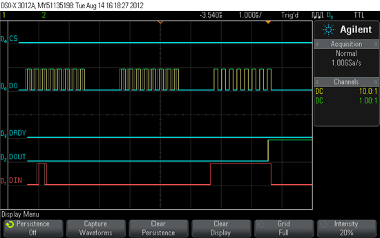
    Can you please provide oscilloscope shots of the SPI connections: SCLK, DIN, DOUT, CS during the RREG command sequence?  This will allow us to check for timing problems.

    Thank you and Best Regards,

    Luis

  •  

    Hello Luis,

    Thank you for your helpful feedback. I took your advice and tried to clear the output register by reading the current conversion, yet the response did not change. The screen shot shows no response from the device (please see bellow). Swiching to continous read, I dot get correct conversion though. Please let me know what you think.

    Regards,

    Hamid


     .  I took your advice and tried to clear


  • Hi Hamid,

    It appears the SCLK frequency being used is around 4 MHz. The ADS1248 allows a maximum SCLK frequency in the order of 2.048MHz.  If you lower the SCLK frequency, does this solve the problem?

    Thank you and Best Regards,

    Luis

  • Hi Luis,

    I changed the frquency  as well, but I get the same results. The data sheet says when operating at 2kSPS, SCLK period cannot exceed 4.2us so 2 MHz should be all right for this sampling rate.  Everything is set to the defualt values theough, since the register values have not been over written yet.  Delaying the consecutive writes to registers also did not help.  Are there any sample code that I can look at to find out the standard way of reading or writing to the registers here? 

    Kind regards,

    hamid 

    int main() {
        float Va2d; 
        spi.format(8,0);                 // 16bit spi polarity(0,1,2,3)
        //spi.frequency(4096000);          // spi freq 4.096MHz
        spi.frequency(2048000);      // ADS1248 max allowed freqeuncy 2.048? 
        DRDY0 = 0; 
        RESET0 = 0;                      // reset the device
        cs = 1;
        wait(2);
        cs = 0; 
        RESET0 = 1; 
        DRDY0 = 1;
        START1 = 1;
        DRDY0 = 0;
        spi.write(WAKEUP);
        spi.write(SELFOCAL); 
        spi.write(SYSOCAL);
        spi.write(SYSGCAL); 
        spi.write(SYNCC);    
        
        spi.write(SDATAC);                  // to read other registers than data, stop readining data continously  
        wait(
       // read and write MUX0
        spi.write(0x40);                    // writre to  MUX0 
        spi.write(0x00);                    // number of bytes - 1
        spi.write(0x01);                    //    BCS1:0 (current) MUX_SP2:0 (positive input) MUX_SN2:0 (negative input) ex: 0x29 = +AIN5, -AIN1, AIN0=01, AIN3=19, AIN4=21, AIN5=29
        // clear the buffer 
        spi.write(NOP);
        spi.write(NOP);
        spi.write(NOP);
        // now read back the register 
        spi.write(0x20);                    // read MUX0 regiter back; 
        spi.write(0x0);
        int MUX0REG = spi.write(NOP);       // read MUX0 regiter back;  
        pc.printf(" MUX0 1byte register contains 0x%X \n\r", MUX0REG);   
        
        // VBIAS : use defult (bias voltage not enabled)
      // configure sampling rate etc.
        wait(0.5);                      // wait 64 oscillator clock before initiating another write 
        spi.write(0x43);                // writre SYS0 register to do 1000 sps 
        spi.write(0x0);                // number of bytes - 1
        spi.write(0x08); 
        spi.write(NOP);                 // clear buffer 
        spi.write(NOP);
        spi.write(NOP);
        spi.write(0x23);                               // read SYS0 regiter back; 
        spi.write(0x0);
        int SYS0REG = spi.write(NOP);                // read SYS0 regiter back;  
        pc.printf(" SYS0 1byte register contains 0x%X \n\r", SYS0REG);
  • Hi Hamid,

    The SPI SCLK phase is probably the issue; the data needs to be shifted to DIN on the falling edge of SCLK.  The DIN data needs to be stable on the falling edge of SCLK and change on the rising edge of SCLK. The START and RESET pins must be held high and CS must be low during the complete communication.

    Whenever reading the registers, I typically simply send the SDATAC command and then issue the RREG command.  The SDATAC (x16h) command is 1 byte long and the RREG command is two bytes + the register data; so this should clear the output register.  The SDATAC takes effect on the next falling edge of DRDY.  You may also take a look at the post below. 

    http://e2e.ti.com/support/data_converters/precision_data_converters/f/73/p/170806/626635.aspx#626635

    The code example available is the code used on the ADS1248EVM-PDK with the MMB3 motherboard.This is code runs on the MSP430F449 processor, and contains a lot of things that may or may not be useful.  It may be a little hard to follow as the code runs within freeRTOS.  In particular, you may find that the ads.c code is the most useful.  Please find attached.

    Thank you and Best Regards,

    Luis

    1641.ads1248evm_fwsrc_1.0.8.zip

  • Good morning Luis,

    Chagning the clock pahse did help. Thanks for the tip there.  I can write to the registers, but reading them back is still toublesome. As far as sending command byte  and RREG, I have done it pretty much your way or according to table 22. The MUX0 register does change since I am able to swich to different a2d channels, and do the conversion correctly. I cannot read the MUX0's  content with the following lines though. 

    spi.write(SDATAC); // to read other registers than data, stop readining data continously
    // now read back the register
    spi.write(0x20); // read MUX0   back;
    spi.write(0x0);
    int MUX0REG = spi.write(NOP);
    pc.printf(" MUX0 contains 0x%X \n\r", MUX0REG);

  • Hi Hamid,

    If you could please provide a new updated oscilloscope shot with SCLK, DIN, DOUT, CS with your new SPI settings during the WREG and the RREG routine this will be helpful... When you send the RREG command, does the DOUT provide the register data looking at the oscilloscope?  What results are you expecting and what are you reading? If an schematic is available, please provide a diagram showing the SPI connections CS, DIN, DOUT, SCLK, START, RESET.

    Please also let me know which processor is being used.

    Thank you and Best Regards,

    Luis

  • Good morning Luis,

    The main problem I had was the clock phase which you pointed out earlier. After changing the phase, read and writre problems got resolved.

    Thank you again for the good observation and all the help,

    Hamid