This thread has been locked.

If you have a related question, please click the "Ask a related question" button in the top right corner. The newly created question will be automatically linked to this question.

Differential Analog Front-End to ADC

Other Parts Discussed in Thread: THS4521, ADS1278, ADS8321, ADS1178, ADS1174

What's the difference between the two implementations? One configuration appears to shunt HF and noise, but would allow the opamp to oscillate if induced. The other configuration would provide the same LP filter and also reduce potential for opamp oscillation. Am I viewing these correctly?

According to Jim Karki's work, the two shunt capacitors should be 2x of the differential capacitor. Why is the capacitor pictured below a 1nF (from the THS4521 datasheet), whereas it should be 33pF?

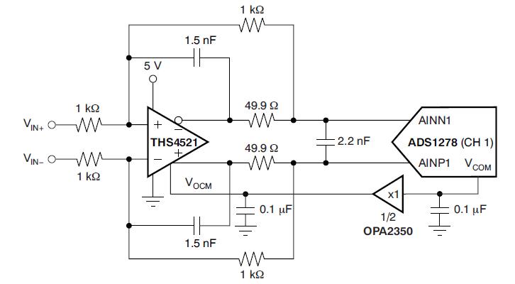
The circuit below puts the capacitors in the feeback loop. This would (1) reduce capacitive loading on the opamp's output, and (2) dramatically reduce gain for increasing frequency, thereby reducing parasitic oscillations. Why is this topology far less published as reference circuits in datasheets, etc?
  • Stephen,

    I think some of the confusion here might be that you're considering these circuits as purely filter circuits?

    These are really just illustrating front-end drive circuitry for a SAR converter (the ADS8321) and a Delta-Sigma (the ADS1278). Between the two architectures we have slightly different care-abouts assuming unbuffered inputs on the ADC silicon.

    Stephen Moore said:
    According to Jim Karki's work, the two shunt capacitors should be 2x of the differential capacitor. Why is the capacitor pictured below a 1nF (from the THS4521 datasheet), whereas it should be 33pF?

    In this case the 1nF cap is just a run-of-the-mill differential capacitor and the 68pF caps are 'charge-wells' to assist the rest of the drive circuitry in charging the SAR sampling capacitor.

    You don't see the bottom circuit as frequently because many delta-sigma converters have the drive circuitry included on chip.

  • Thank you for the response.

    I'm using the ADS1178, which is a delta-sigma type. The ADC is reading two kinds of sensors: The "type-A" sensor outputs a raw value. The "type-B" sensor has internal low-pass filtering. Therefore, if read simultaneously, these sensors do not have coherent phase and magnitude. So, I'm designing a 1-pole filter for the type-B sensor for a total of two poles (mine plus the internal filter equals two poles). Then, the type-A sensor gets 2-poles, and they'll match phase coherency.

    The differential input stage is important because of the nature of the sensors. The sensors will primary operate at Vanalog/2 = Vocm, which is perfect for differential input. It is also what is implemented on the ADS1174/8 EVM.

    The bottom schematic appears superior. The capacitors in the feedback loop have low impedance to high frequency, therefore preventing parasitic oscillations. The top schematic forces the amplifier to drive a capacitive load. I was curious since the circuits have similar parts count (maybe a few extra resistors and small capacitors), why literature favors the top circuit?

  • Stephen,

    You might say the top circuit is more explicit because it shows the pair of 68pF 'charge well' capacitors and this is most likely how it would be illustrated in literature just to highlight the circuits intentions. Adding similar charge-well capacitors to the bottom circuit could be argued as 'most correct' from a purist point of view and may gain you some performance improvement in very extreme situations, you probably would not gain much though. We've taken that particular circuit into the lab in the past and in simulation and proven that the 'charge-well' caps are not necessary in this particular situation. The second circuit also has the active filter you mentioned, but it should be considered an addition to the circuit not a relocation of the same capacitors that are in the upper schematic.