This thread has been locked.

If you have a related question, please click the "Ask a related question" button in the top right corner. The newly created question will be automatically linked to this question.

ADC12D1600. Fs/4 spur in DES mode.

Other Parts Discussed in Thread: ADC12D1600, ADC12D1600RF, ADC12D800RF, LMH6554

Hello.

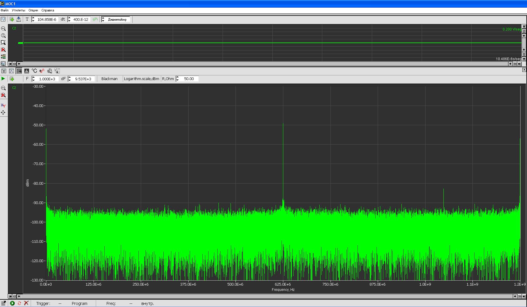
I have developed digitizer based on ADC12D1600. ADC works in DES mode with sampling frequency Fs = 2,5 GHz. ADCs input mode is DC-coupled with FSR 1000 mV. Data outputs are not demultiplexed (Not-Demux DES mode).

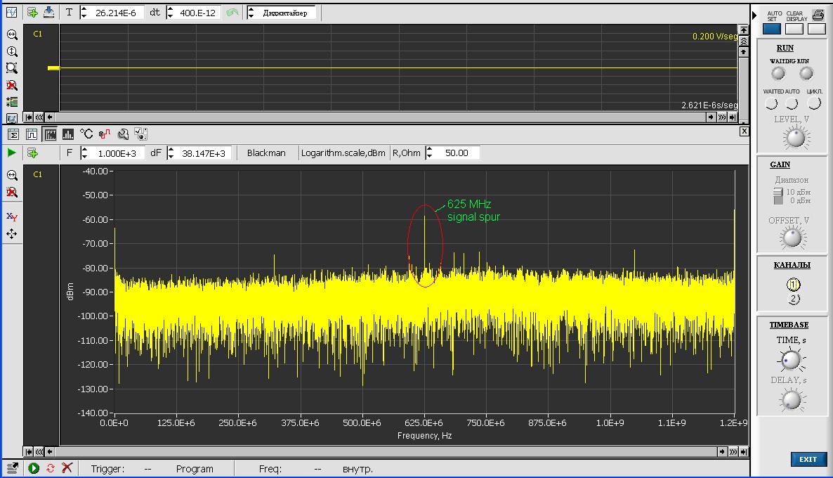
On a spectrogram, that I have gotten from my device I see parasitic signal spur on 625 MHz, which is 1/4 of my sampling frequency. When I change sampling frequency to Fs = 1,25 GHz appears 312.5 MHz signal spur. Spur level is about - 55 dBm. I think, it's not induced on ADC inputs (although I could be wrong). Full scale range and DES timing adjusting lowers aliasing frequency (Fs/2 - Fin), but doesn't affect on Fs/4 signal spur.

I found a datasheet in which is making comparison RF and not-RF versions of ADC12D1x00. As I see on this picture each of AD12D1x00 ADC channels (I and Q) consists of two subchannels (I1 & I2 and Q1 &Q2). Is that means that I and Q channels works in their own interleaved mode on Fs/2 frequency? That may be cause of Fs/4 spur appearing in DES mode...

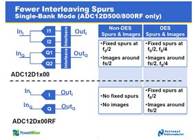
Here is said, that ADC12D1x00RF has fewer interleaving spurs in DES mode on Fs/2 and Fs/4. So, should I use RF ADC instead of not-RF version to cancel problem with Fs/4 spur in DES mode? Or, may be I did something wrong during design process. Please help me to solve this problem.

Thank you.


  • I removed input resistors and leave ADC I-channel inputs floating.
    Then, I made measurement in DES mode with Fs=2.5 GHz, and had got this:

    As you can see all induced noise and differential amplifiers own noise is canceled. But 625 MHz parasitic spur is still here.
    What may be a cause of this?

  • Hi Deus,

    Sorry you are trying to debug this issue.  Let me show you the source of the Fs/4 spur first and then consider what can be done about it.  -55dBFS sounds a little high compared to what I typically see, but it is possible, especially with the DCLK coupling in addition to the offset mismatch and the sub-converter clock.

    There are three sources which contribute to the Fs/4 spur in DES Mode for your application:

    • Offset mismatch between sub-converters in a 4x interleaved data converter.  The ADC12D1600 has actually 2x interleave per channel, so in DES Mode, this totals to 4x interleave. 
    • Sub-converter clock.  Each channel is actually being sampled at Fs=625Msps, which also lands at Fs/4 for the DES Mode (Fs=2500Msps)
    • DCLK: Non-Demux DDR Data Clock (DCLK) is running at 625MHz, which lands at Fs/4 for DES Mode

    Regarding the 'Fewer Interleaving Spurs' image you pasted in, let me clarify a little.  The 'RF' parts have better distortion than the non-RF parts, but they still have this issue with the spur at Fs/4, since it is due to parasitic clock coupling.  For example, the ADC12D1600RF will still show a spur at Fs/4 in your system without any input. 

    Regarding the ADC12D800/500RF having fewer interleaving image spurs, that is true, but it will only affect the spurs at Fs/2-Fin, Fs/2-H2, Fs/2-H3, ... Also, the faster product, the ADC12D800RF, will only run at maximum 1.6Gsps in the interleaved mode, and you need 2.5Gsps for your application, so that product is not a good fit.

    To minimize the Fs/4 spur:

    • Calibration should minimize the offset between the ADC sub-converter banks.  From the FFT, it looks like you calibrated, but please just verify that you did. 
    • If you use a Demux DDR DCLK, then the Fs/4 spur contribution from the DCLK will move to Fs/8.  Depending on your application, I'm not sure if this is acceptable or not?
    • To minimize the contribution from the sub-converter clock, it's possible that reducing the level of the clock at the CLK+/- inputs may help, but I need to check this idea in the lab.

    There are a couple keys to solving this issue: to determine which contributor is the main culprit and see what may be done to reduce its level, and to understand what the minimum acceptable level for your application is.  Can you tell me any more details about your digitizer application performance requirements?

    Kind regards,

    Marjorie


  • Hello, Marjorie.
    Thank you for response. I'm sorry for a little delay with my answer because I'm now taking part in exhibition with our new devices and could not check operatively your assumptions about Fs/4 contributors. But after couple of days I'll come back to work with digitizer board and will continue my investigations of that problem.
    Now, just want to clear some issues and ask one more question.

    Answering your questions:
     - I do calibration every time before starting capturing data. When I start ADC calibration, analog signal is presenting on I and Q channel inputs.
    So, if I even disable my differential amplifier LMH6554, which is sourcing signal for ADC, there will be some voltage level on ADC inputs, because of DC-coupling and feedback resistors divider of the amplifier. 
    - Multiplexed mode is not acceptable for me because Id and Qd buses are floating.
    - Do I rightly understood, I need to reduce differential level of the PLL output clock signal, which is sourcing my ADC?

    Some words about my digitizer.

    I configure ADC to work in such way:
     - first of all, because of high power consumption I leave ADC in power down mode between measurements. So, every measurement starts with setting PD mode off;
     - after that, I turn on ADC test signal and make delay for 1 ms,
     - than, I start calibration and wait for it's finished;
     - than, I wait for LVDS reciver in FPGA becomes to be locked on right data/clocke phase.
     - after that, I switch from test signal back to normal inputs and make another 1 ms delay.
     - start capture data from ADC to memory.
     - after finish of capturing I set ADC PD mode back ON.

    What do you think about this sequence? Maybe I do something not exactly in a right way.

  • Hello. Do you forget about me? Could anyone help me further?

  • Hi Andrey,

    I'm sorry to neglect your debug issue for a little while!  If you send me your contact info, I can send more info regarding GSPS ADC spurs: sources and methods of mitigation.  All data converters have spurs which are the results of non-linear effects in the conversion process; understanding these is the key to dealing with them.

    Leaving the LMH6554 on the input of the ADC could cause some offset; however, I expect this to simply show up as a spur at DC and not contribute to the one you are seeing at Fs/4.  Changing the level of the Sampling Clock (CLK+/-) may affect the level of the Fs/4 spur; however, I do not expect this to affect it so significantly as to be able to reduce the spur level from what you are seeing ~55dBFS to what I typically see ~75dBFS.

    Your configuration sequence looks very reasonable.  Do you monitor the CALRUN signal to verify that the calibration procedure has completed?  If you are already doing this, then it seems that you are able to verify that the calibration has taken place correctly.  The only other thing I can think of to try on your setup would be to power the LMH6554 down, calibrate the ADC, and take an FFT with no input to explore the source of the unexpectedly large Fs/4 spur.

    Using a Demux DCLK was the other option, but if you cannot do that, then it may not be possible to reduce the spur any further.  I understand that this is for a digitizer application.  What kind of signals are you digitizing?  Is there any possibility to plan around this spur?

    Kind regards,

    Marjorie

  • Hello, Marjorie.

    Thank you for reply. I need a few days to check yours ideas. After this, I'll write back to you.

    My personal e-mail for contact is andreyboltovsky@gmail.com

    I monitor CALRUN and it goes low after calibration is finished. So I think, calibration is finishing successfuly.
    My device is a common measurement instrument, for digitizing any kind of signal from DC to 1 GHz with dynamic range of 70-80 dB. So, I can't ignore or plan around this spure.

    Regards, Andrey.

  • Hi Andrey,

    It sounds like your system is successfully calibrating, which is good.  When using the ADC12D1600(RF) in DES Mode, there is no mode to completely remove the Fs/4 spur.  This is possible to accomplish on the ADC12D800RF, but like I mentioned before, this has a maximum Fs=1.6Gsps sampling rate and your application requires 2.5Gsps, so we are stuck between a rock and a hard spot...  I'm open to discussing solutions; feel free to give me a call.

    Kind regards,

    Marjorie

  • Hello, Marjorie.

    Now, I'm stuck with calibration procedure of my digitizer. I have one small question about I and Q FSR (full scale range) settings. So, I decided not start new topic and ask it here.

    But, first of all, I have some good news, concerning Fs/4 spur problem. I experimented with different ADC settings and self-calibration modes. And, after I've done two things, Fs/4 spur became significantly smaller, about 68 - 78 dBm on both channels (you can see my early posts, it was about 55 - 65 dBm).
    This things are:
    1) I've set OVS bit to zero. It lowers differential voltage level of LVDS outputs.
    2) I've stop doing ADC self-calibration before every measurement. Now I make it once, only after ADC setup. There is only one issue, now I need to monitor ADC temperature and repeat self-calibration if it significantly changes. Especially, after power-up, when it rises very fast. 
    I'm not about to stop my further investigations of this problem. I hope, I can make Fs/4 spur even lower than now. 

    Now, my question about FSR setting.
    I calibrate I and Q channels OFFSET and FSR, working is DESI, Not-DEMUX modes.
    When I change I and Q offset setting thru ADC 2h and Ah registers, I see difference between I and Q data outputs arrays, so I can change I and Q offsets in such way, that I and Q data will be equal. Here is all OK.
    But, when I try to make same thing with I and Q FSR setting (thru 3h and Bh registers) I see that I and Q data arrays always changes simultaneously, even if I changed only one FSR (I or Q). In a simple words: I change only I-FSR, but Q output data changes too, along with I data. And vice versa. 
    Why this is so? Is it such feature of DESI (DESQ) mode?

    With best regards, Andrey.

  • Hi Andrey

    I did a quick check on the bench to verify the behavior in DES-I mode.

    What I see is that when I change the I or Q channel FSR setting, at first the channels do have different FSR settings. This is observed by the large Fs/2-Fin spur that shows up due to the gain mismatch.

    If I then run a self-calibration, that process adjusts the I and Q channel internal settings such that they have matching FSR and the Fs/2-Fin spur is minimized. The FSR register values stay where I had set them, so the adjustment is made to internal calibration values only.

    So the behavior you see is due to the way that calibration works when the device is in DES mode. If you want to make any adjustments to I versus Q FSR, you will need to do that after running self-calibration. If self-calibration is then run, it will effectively un-do any changes you have made to FSR.

    I hope this is helpful.

    Best regards,

    Jim B

  • Hello, Jim.

    Thank you, for reply. Now, I understand what happens. I really started self-calibration every time after setting ADC registers.
    Unfortunately, even after self-calibration there is a little difference between I and Q data arrays. But, Fs/2-Fin spur is about - 70 dBm. It suits me for now. 
    Thank you for help.