


Dear all,
We’ve got a question concerning the use of TI ADS8344NB 16-Bits Analog to Digital Converter.
In our design, the ADS8344 is used to monitor a few thermal sensors and the board power supplies (3.3V) through 51 ohms serial resistors (VCC_CONV=5V and MES_V5BOOST=3V):
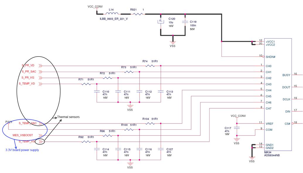
One of the boards is currently down after a few weeks of operations, and a failure has been identified on ADS8344NB, which is driving much more current than others (around 300mA on 5V power supply), especially on Vref input, which I guess is only a reference voltage and should not driving any current.
We analyzed that during board power up, the power supply sequencing may cause an electrical stress over the maximum ratings during about 1ms, because P3V3ADC input (Green) is faster than the VCC_CONV power supply establishment (purple):
According to the ADC internal design, what can be the effect of such stress conditions on ADS8344NB? May this be the root of our problems or have any other ideas?
