This thread has been locked.

If you have a related question, please click the "Ask a related question" button in the top right corner. The newly created question will be automatically linked to this question.

DAC8581 problems

Other Parts Discussed in Thread: DAC8581, OPA627, DXP, DAC8734

Hi everyone,

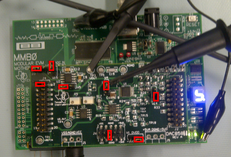
I have a DAC8581EVM board with a DAC8581 unit. I have designed an VHDL interface on a FPGA in order to introduce the SPI data. When I connect the development board with the FPGA and the power supplies, I get a wrong output voltage.

Here are the connections I have implemented:

ANALOG POWER SUPPLIES
======================= 
Vcc <= +11.70 V (to AGND)
Vss <= -11.70 V (to AGND)
AVdd <= +5.10 V (to AGND)
AVss <= -5.10V (to AGND)
AGND <= AGND 

DIGITAL POWER SUPPLIES
======================= 
+5VD <= +5.10V (to DGND)
+3VD <= +3.3V  (to DGND)
DGND <= AGND

DAC DATA (J2)
============
J2-1 <= CSn;
J2-3 <= SCLK
J2-11 <= SDIN
J2-14 <= CLRn

When SDIN <= "4000", the output voltage at TP5 = 3.5 V, but the datasheet indicates that it should be 2.5V.  With other values there are discrepacies too, as shown in the table below:

SDI Value                   Expected value               Obtained value                 Error 
============         ============               ===========                  ====

0x7FFF                                 5V                                    4,02V                          19,6%
0x4000                                 2,5V                                3,49V                           39,6
0x0000                                 0V                                    0V                                  0%
0xC000                                 -2,5V                              -2,2V                             12%
0x8000                                 -5V                                  -4,6V                              8%


I expected that a 16-bit DAC should be more accurate, so I think that I am doing something wrong. If so, this mistake could be in the connection, or in the data transfer.

- Connections are explained above.

- Jumpers : all the jumpers are set as the default implementation (datasheet).

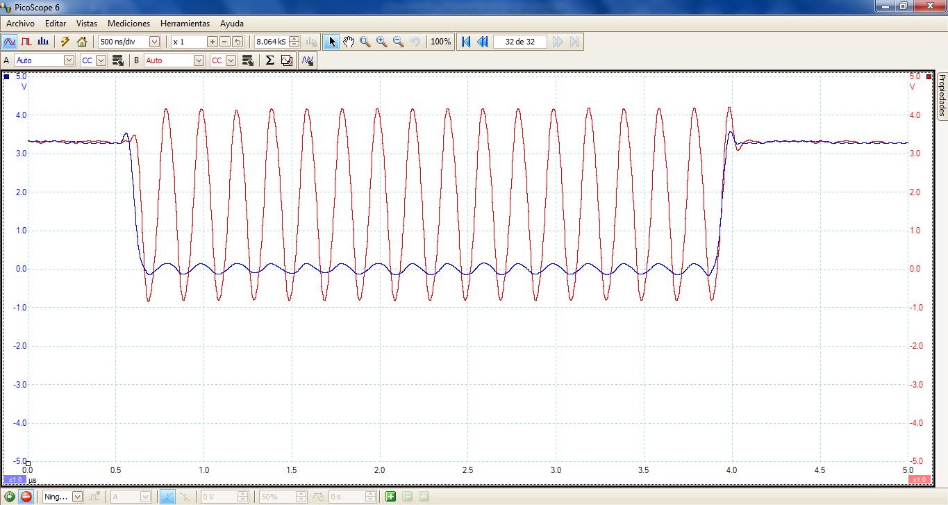
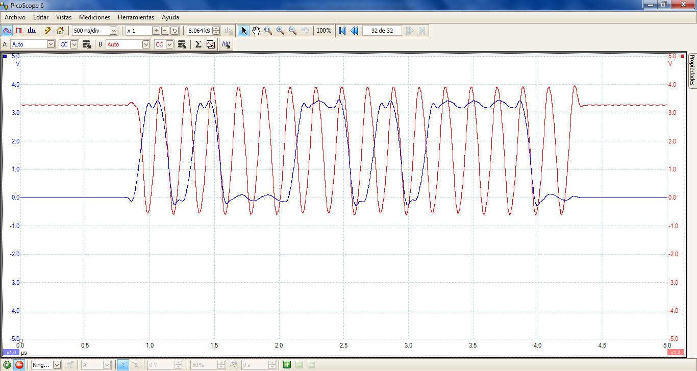
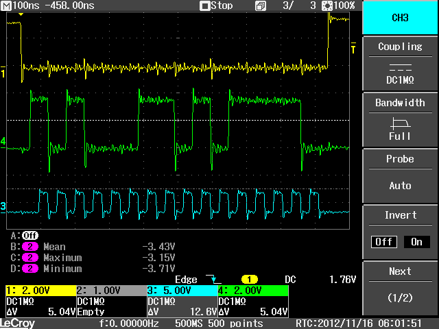
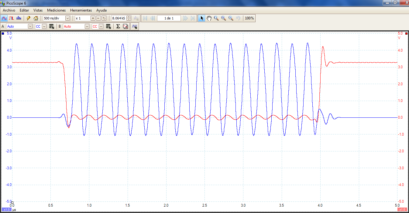
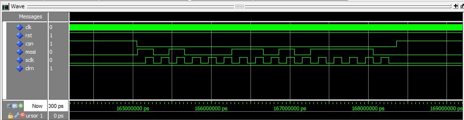
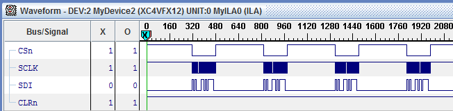
-Below there is a graphic to show the SPI Data transfer through SDI pin. The data trasnferred is A35E hex. 

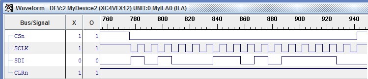
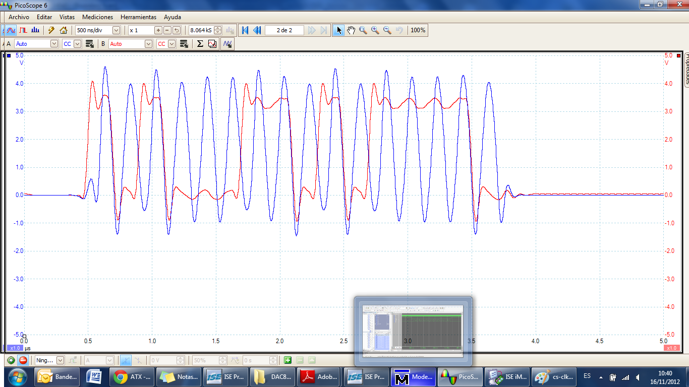
with SCLK frequency = 10 MHz. Below a multiple conversion is performed (the SDI data is always the same), sending data @ 200 Ksamples/s:

If anybody has worked with this DAC, or can help with the information given and the DAC datasheet, I would be very grateful for your help. If any additional information is needed, just ask.

Thank you everybody in advance,

Alberto

  • Hi Alberto,

    You SPI timing looks to be correct - you're at least using the right clock edge. Seeing a direct oscilloscope captured would be more useful for looking at the complete timing specifications but I don't think that should be the issue here.

    If I've interpreted your connections correctly you have +/-5.1V on AVSS and AVDD of the DAC8581 with +/-11.7V for the rest of the board's supplies. Are you providing an external reference? If not, you should verify the voltage present from the reference at TP4 or pin 1 of W4 and correlate that to your expected values, sometimes the trim resistor and potentiometer aren't set correctly from our manufacturers. Another item of note is that with 5.1V supplies you are probably not going to be able to reach 5V because of the overhead for the internal buffer. I wouldn't expect to see you rail at 4.02V, however. Keep in mind that W15 is a gain setting resistor for the output from the OPA627.

    Your results do not follow any clear trend, and you should see much better results from this device. Check the reference voltage you have present and we'll go from there.

  • Hi Kevin,

    Thank you for your quick response. 

    I am not using an external reference at TP1. W4 jumper position is 1-2. Voltage at pin 1 of W4 is 4.99 V, and if I understand the datasheet this voltage should be 5V, so it is correct.

    I don't think is an SPI timing problem either, but it could be anywhere. Is there any consideration that must be taken related to SPI timing? (in addition to the clock edge)

    According to the datasheet, when the input is 7FFFh, output voltage should be Vref (i.e. 5V) , how comes that I won't be able to reach 5V? What voltage range would I be able to reach?

    Thank you very much,

    Alberto

  • Alberto,

    Thank you for looking into your reference voltage. The output range of the device is primarily limited by the reference, as in the maximum range that the device could ever achieve is +/-Vref. If the supply rails are not sufficiently above the reference voltage, the output buffer will begin to limit the output range because the buffer is not a rail to rail amplifier. There is roughly 500mV of overhead necessary on the supplies to achieve +/-Vref output range. There is a small note concerning this on page 3 of datasheet in the electrical characteristics table; "Vref up to 5.5V, when AVDD = 6V, AVSS = -6V"

    Using a MMB0, our evaluation motherboard, with a DAC8581EVM and nearly the same supplies you have described (+/-12V on VSS/VCC and +/-5V for AVDD and AVSS) I can realize an output range of roughly -4.76V to 4.68V, which is aligned with the comments in the datasheet. If you ordered an EVM-PDK, you should also have an MMB0 and can use DXP - our DAC evaluation software - to exercise the DAC and verify your EVM jumper settings & supply configurations before applying your FPGA to isolate potential jumper problems.

    I understand that your jumper settings should be to the EVM User's Guide defaults, but to solidify your jumper settings, here is a picture with the jumper configuration I used in my setup:

    J3 => 2-3 Position
    W15  => Uninstalled
    J4 =>J4.1 short to J4.2
    W5 => 1-2 Position
    W4 => 1-2 Position
    W14 =>2-3 Position 

    W1 and W14 can be set according to your own needs for interfacing your FPGA. If you use the EVM with the MMB0 and DXP, though, make sure W14 is in the 2-3 position as shown in the image above.

  • Alberto,

    One more thing, the timing diagram and requirements documented on page 5 of the datasheet are the rest of the parameters of the serial interface that we may need to check out. If your jumper settings match whats in the previous post try to get oscilloscope captures of the 3-wire interface and share the time division with us. 

  • Hi,

    Thank you so much for your help, Kevin.

    Here are timing diagrams you asked for. 

    Below is the CS-SCLK diagram:

    And below is the timing diagram SCLK-SDI:

    The data sent in the image is A35E.

    I have checked the jumpers and they are the same as yours except W14, which is set at 1-2.

    Thank you very much,

    Alberto.

  • I forgot to say that SCLK frequency is set @ 5MHz.

    MAybe you can tell me the output with this data and we can check it with mine. As I said in the first post, the biggest error is around SDI = X"4000".

    Alberto.

  • Alberto,

    I don't see anything wrong with your serial interface captures. Below is a capture from the serial transaction I have used to stimulate the DAC. You may want to try inverting your clock polarity since the datasheet illustrations use polarity 0. I've seen problems come up in the past with other devices due to similar issues.

    0xA35E results in a -3.43V output, which is a little low compared to the -3.6V I would have expected to see. I believe that there is an internal buffer on the reference input that is limiting the reference actually used internally due to the supply configuration of the device. I see similar issues with 0x4000 generating a 2.3V output rather than 2.5V. If the reference is scaled back to 4.5V or lower I see much more linear and expected behavior which gives credence to the notion of an internal buffer being present on the reference. Since this is a bit of an old part it is hard to confirm whether this buffer is present or not.

    Try flipping the clock polarity and let me know your results. Also, describe how you have the power supplies connected if that does not correct the issue. 

  • Hi Kevin,

    I have performed the change you suggested. Here is the new simulation of the SPI transfer:

    And below the transfer with the oscilloscope:

    When sending X"4000" through SDI, with the voltages detailed in the first message of this post and SCLK default value set to 0, I have obtained the following results:

    TP3: 4,15 V

    TP5: 8,3 V (since W15 is ON)

    Obviously, these results are really higher than the expected ones.

    When repeating the previous procedure, with SCLK default value set to 1, I have obtained the following results:

    TP3: 2,08V

    TP5: 4,17V

    When repeating the previous steps for SDI = X"2000", the results obtained are:

    SCLK DEFAULT VALUE = 1 => TP3 : 0,52V, TP5: 1.04V

    SCLK DEFAULT VALUE = 0 => TP3 : 1,04V, TP5 : 2,08V

    It seems that depending on the SCLK default value, the output gets a value or its double, but it doesn,t make any sense beacuse in the datasheet seems to say that this default value in the SCLK signal is not important. And it's obvious I have got no linearity in the device.

    Can you tell me the voltages you obtain with this input voltage or another?

  • Sorry, the simulation graph has not been sent correctly:

  • Alberto,

    There has to be something else at play here. You jumper settings are identical to the setup here and your digital signals do not seem to have anything wrong with them, SCLK should idle low though - in my tests at 5MHz with SCLK idling high the device does not respond at all. It's difficult to measure by eye but make sure that you have 20ns between CS falling and the first rising SCLK. Also ensure that the values on DIN are setup for at least 5ns before the rising clock edge and are held at the correct value for 5ns after the rising clock edge. It looks like you're meeting these requirements but a scope measurement would be more accurate.

    I've tried playing around with the digital words you're sending to come up with a bit-shift that may be producing the errors you're seeing but it just isn't there.

    Your initial post indicated that sending 0x4000 to the device yielded 3.49V output under your initial configuration with SCLK idling high. In your most recent experiments now you see 2.08V on the output when SCLK is idling high. What has changed? Is this maybe a grounding problem? Share your power supply connections (where is each supply connected, how does each supply share ground connections) and exactly how you're measuring the output voltage (where is the ground clip, what are you using to get the voltage measurement). Maybe even include a picture.

    In your initial post the negative voltages track almost as expected but the positive voltages are all over the place. Additionally for best linearity you should consider reducing the reference voltage to allow for more headroom inside the device, this is a worthwhile experiment anyhow. You need 300mV-500mV of headroom between the reference and the DAC supplies to be able to swing +/-VREF. If nothing else, better linearity will help us in debugging the situation if it's just a problem with your digital words.

    In all of my tests the device responds as expected when output rails and reference rails are taken into account.

  • Hi Kevin,

    Thank you for your support :)

    Here are good news and bad news, but we are getting a bit closer I think.

    I checked again the values of the output voltages and you were right, somehow the other day I made a mistake and the voltages I obtained were wrong. I have repeated the measurements and here are the results:

    1)                          Input value              Output voltage                                          Input value              Output voltage
                                 =========             ============                                       =========             ============
                                      7FFF                             4,77 V                                                     F800                              -0,3 V
                                      4000                             3,58 V                                                     F000                              -0,6 V
                                      2000                             1,78 V                                                     E000                              -1,2 V
                                      1000                             0,89 V                                                     C000                              -2,4 V
                                      0800                             0,44 V                                                     8000                               -4,8 V
                                      0000                                   0 V
                                     
            Now the voltage of 4000 is aprox the obtained in the first measurements.
            We can see that there is some linearity in the data obtained. However, the slopes for positive and negative values are different.

    2) The previous behaviour is not the expected, but it could be fixed by multiplying the output by some constant. So then I performed the same test with the intermediate values, and here are the results:

                                  Input value              Output voltage                                          Input value              Output voltage
                                 =========             ============                                       =========             ============
                                      6000                             4,16 V                                                     E800                              -0,75 V
                                      3000                             2,08 V                                                     D000                              -1,5 V
                                      1800                             1,04 V                                                     A000                              -3 V

          As you can see, there is again some linearity. But there is no linearity with the data obatined in 1) !!!! The data expected would have been:

                                  Input value              Output voltage                                          Input value              Output voltage
                                 =========             ============                                       =========             ============
                                      6000                             5,4 V*                                                     E800                              -0,9 V
                                      3000                             2,7 V                                                     D000                              -1,8 V
                                      1800                             1,35 V                                                     A000                              -3,6 V

         *This value never could be reached because of the reference voltage, it should be smaller than 4,77 V.

    So here we are now, does this values make any sense to you? Do they match with those ones you obtain?

    Now I'm answering your questions:

    - Analog power voltages come from an switching pc power supply (atx). The connections are the one I told you in the first post.

    - Digital power voltages come from a Xilinx ML403 board. 

                      · 5 V => 5 V bank (ml403 connector J3-pin1)
                      · 3.3 V => 3.3V bank (ml403 connector J3-pin7) (W1 is set to 2-3)
                      .DGND => GND (ml403 connector J5-pin5)

    - Analog and digital grounds are tied together 

                       · ml403 connector J5 pin 11 is connected to dac8581evm connector j4 pin 17)

    - Data signals (refered to dac8581evm)

                       · CSn : connector J2 pin 1
                       · SCLK : connector J2 pin 3
                       · SDIN: connector J2 pin 11
                       · CLRn: connector J2 pin 14 

    Voltage at W4 is 4,99 V.

    Since now we are obtaining some kind of linearity, I don't think there is a connection problem, but I may be wrong.

    I hope this may help. Anything else you need, please ask.

    Thank you,

    Alberto.

  • Hi Kevin and everyone,

    Thank you first, Kevin, for all the support you are giving to me, I really appreciate it.

    For all the 'new' people, I'm going to expose my situation. As I described in this post, I can't achieve the performance I desired from the DAC8581. In the previous message, I described the behaviour of this DAC.

    I work in an engineering company and we have a project which needs many items of this DAC. We estimate that we can need hundred of items per year. But if we can't get the performance desired, we will need to choose other DAC or maybe another brand. We have worked in previous projects with other TI DACs, like DAC8734, and we are very satisfied with the performance obtained, but this time we don't.

    I would really appreciate any help that you could give to me.

    Thank you in advance,

    Alberto.

  • Alberto,

    Sorry for the lack of responses here. With the Thanksgiving Holiday in the US last week I was out of office and have been spending a lot of time catching up on things today. I will be giving this another look again soon.

  • Alberto,

    Finally trying to return to this. Have you made any progress on your end? This part has questionable linearity specs but it shouldn't be as bad as what you've been seeing by my results.