This thread has been locked.

If you have a related question, please click the "Ask a related question" button in the top right corner. The newly created question will be automatically linked to this question.

Problem with ads1247 and pic18f4550

Other Parts Discussed in Thread: ADS1247, ADS1118

Hello, i´m working with the ads1247 and a microcontroller pic 18f4550 and i have a problem. First i program the ads registers with the following values:

mux0=0x01

VBIAS=0X00

mux1= 0x60

SYSO=0x71

IDAC0=0X07

IDAC1=0X01

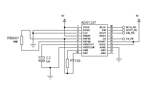
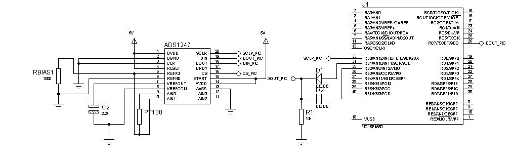
I want to work with a rtd in three wire connection with hardware compensation, therefore the ads´s pin are conected in the following way:

DVDD=5V, DGND=GND, CLK=GND, RESET=5V, REFP0=REFN0=RBIAS, VREFOUT connected to a .2.2uF capacitor and thisone connected to VREFCOM, VREFCOM=GND, AIN0 and AIN1 connected to RTD, AVSS=GND, AVDD=5V, (START, CS, DRDY, DOUT, DIN, SCLK) connected to the microcontroller.

The thing is that after i write the registers i´m able to read them and i can see they are correctly loaded. After this i start a conversion and when the start´s bit returns to 0' all the registers are erased lather if the start´s bit returns to 1' i can read again the correctly values of the registers. Even if the START is allways in 1' the only data that received the pic is 128 in the MSB of the data conversion. If i want to messure the RBIAS voltage using a voltimeter the same thing happen again (all the register are erased). I am reading the data (registers values and temperature convertion) in a lcd display connected to the pic. Next i attached the firmware of the pic in c language.


#INCLUDE <18F4550.H>
#fuses INTRC_IO,PUT,VREGEN,NOWDT,NOPROTECT,NOLVP,NODEBUG
#use delay(clock=4000000)
#use spi (master, bits=8 , di= pin_b0, do= pin_c7, clk=pin_b1, msb_first , force_sw)
#include <lcdpf.c>
#define cs pin_a0
#define start pin_a3
#define ready pin_a1

int dato_spi1[]={5,6,7}, dato_spi2[3];
float dato;
int i,j,k,l,m,n,flag=1;
void start_ads()
{

output_low(cs);
spi_xfer(0x06); //Reset
delay_ms(3);
spi_xfer(0x16); //SDATAC
spi_xfer(0x40);
spi_xfer(0x03);
spi_xfer(0b00000001);
spi_xfer(0b01100000);

spi_xfer(0b01110001);
spi_xfer(0x4A);
spi_xfer(0b00000001);
spi_xfer(0b00000111);
spi_xfer(0b00000001)
output_HIGH(cs);
}

void main ()
{
lcd_init();

output_HIGH(cs);
set_tris_a(0b00000010);
set_tris_c(0);
set_tris_b(0b00000001);
start_ads();

while (1)
{

output_low(cs);
delay_ms(10);
spi_xfer(0x20); 
spi_xfer(0x03);
i=spi_xfer(0xff);
j=spi_xfer(0xff);
k=spi_xfer(0xff);
l=spi_xfer(0xff);

spi_xfer(0x2A); 
spi_xfer(0x01);
m=spi_xfer(0xff);
n=spi_xfer(0xff);
delay_ms(10);


output_high(START);
Delay_ms(1);
output_low(START);
Delay_us(30);

spi_xfer(0x12);
delay_ms(300);
dato_spi1[0]=spi_xfer(0xFF);//MSB
dato_spi1[1]=spi_xfer(0xFF);//MID BYTE
dato_spi1[2]=spi_xfer(0xFF);//LSB
output_high(cs);

lcd_gotoxy(1,1);
printf(lcd_putc,"mux %2x te %2.2f ",i,dato);
lcd_gotoxy(1,2);
printf(lcd_putc,"mux %2x te %2u ",j,dato_spi1[0]);
lcd_gotoxy(1,3);
printf(lcd_putc,"mux %2x %2x mux %2u ",k,m,dato_spi1[1]);
lcd_gotoxy(1,4);
printf(lcd_putc,"mux %2x %2x mux %2u ",l,n,dato_spi1[2]);
output_low(pin_a2);


}
}

Sorry for my bad english, i´m from Argentina. I hope you can helpme. Best regards

  • Alfredo,

    Welcome to the forum!  The START pin can be considered a power down pin.  When it is low, you are effectively shutting down the part.  The START pin must be high for all conversions and communication to the device.

    Best regards,

    Bob B

  • Hi Bob. Thanks for your answer. I connected the START pin to 1´all the time and i could read a conversion only if i write the register VBIAS=0x01. Why do you think this happens? Don´t forget that i am using this device only to measure rtd. If i write another value in VBIAS the conversion showme the MSB=0X80 and the rest of the bytes are 0. Another question, do you know why i can´t measure the voltage in Rbias with a voltimeter or an osciloscope?

    Best regards

  • Could you tellme what is the porpouse of the vbias register? Should i use it? and how must i configurate it if i am working with a rtd in three wire connection?. Right now i am probing the device with Vbias=0x00h and mux1=0x20h and i read the conversion with the msb=0x7h and the rest bytes are 0xffh could you helpme please?

  • Alfredo,

    The VBIAS register is used to establish a bias voltage for thermocouples so that it is within the common mode input range of the PGA.  For RTDs you would not use the bias voltage.

    Can you send me your schematic?  Also, can you send me some scope shots of your communications?  For RTD measurements, you establish a reference voltage through a bias resistor that is connected in series with the RTD.  One thing is to make sure that the internal reference is turned on, even though you use an external reference.  The internal reference is used to establish the IDAC current.

    Best regards,

    Bob B

  • Hi Bob, Here is the schematic of the design i am using. Unfortunatlly i can´t attacht a scope of the comunication because as i told you when i connect the osciloscope, all the signals go to zero. Now I have the follow configuration of the registers:

    MUX0=0X01. VBIAS=0X00. MUX1=0X020. SYSO=0X71. IDAC0=0X06. IDAC1= 0X01. given that i can read the registers using the RREG instruction, i can assure you that they are correctly written. And the Microcontroller allways receives MSB=0X7F and the rest is 0xff and the voltage across the Rbias is 3V and across the RTD (between AIN0-AIN1 at 25°C) is aprox. 100mV. I want to meassure between 0 and 50°C. If i am using only one RTD connected in three wire configuration between ain0 and ain1, Should i use the IDAC2 source?

    Take notice that Avdd=Dvdd=5V, Is ok to do this?

    Best regards

  • Alfredo,

    You need to create a current path to ground.  You need to connect the RBIAS/REFN0 connection to ground.  I think what may be happening is when you turn on VBIAS a ground path through the input is created.

    Best regards,

    Bob B

  • Bob do you think the rest of the registers has the correctly configuration to my project? because I tried with two different ads1247 and both gave me the same answer, so i start to think that the problem may be was in the firmware. What do you think?

    Best regards

  • Alfredo,

    The VBIAS register should be all 0.  To keep things less complicated you should leave the internal reference always on, so MUX1 should be '00100000'.  As I mentioned earlier you must make sure you have a current path and that RBIAS and REFN0 are grounded.  I would double check all your supply/ground connections.

    Best regards,

     Bob B

  • Hi Bob. Today i could check the connections of the device and i could see that the pin RBIAS /REFN0 is connected to gnd , and the registers are configurated as you told me before vbias=0x00 and mux1=0x20, so the project is working as same as allways. I could note that if i change the value of the RBIAS the convertion´s result is the same. I connected a led to the pin DRDY and i could see that the led is the most part of the time off, and later became to 1 just for a very short time. I supposed that pin works exactly the opposite, it will be down when the conversion was ready and the rest of the time would be to 1'. The led´s anode is connected to the pin and the catode is connected to gnd with a resistor. Do you know why is working in that way?. I have DVDD=AVDD=5V and in the p 57 of the datasheet, AVDD=5V and DVDD= 3.3V do you think the problems is in there?

    I attached the final schematic

    Thanks for your answers. Best regards

  • Hi Alfredo,

    One thing I should have mentioned earlier is the START pin must  be high when writing the registers.  This pin is like a power down pin.  It not only powers down the ADC, but you will also power down a portion of the digital.  I would suggest you leave the START pin high until you are fully satisfied with the operation.  After that you can use the power down modes.

    As far as DRDY operation, the pin will only go high when new results are  being updated if you do not read from the device.  When you read data from the device, the DRDY pin will go high until the next updated has been completed then DRDY will go low.

    Best regards,

    Bob B

  • Hi Bob. As i showed you in the schematic I have the START pin connected to 1´all the time. I tried with two different ads1247 and i have the same response from the device. Do  you thing that my problem is in the firmware? In that case which would be my error (my source code is in the beggining of the post)? Did you considered my last question about the source (AVDD=DVDD=5V) ?

    Best Regards.

  • Alfredo,

    I'm sorry I didn't take a closer look at the schematic.  Yes, I see you have START pulled high.  You can use the same 5V power supply for both AVDD and DVDD.  This now takes us all the way back to the beginning in that we need to verify the communication.  The only way to do that is either with a logic analyzer or oscilloscope.  Using an oscilloscope should not short out the output, and is much better for verification as compared to using LEDs.

    Basically you need to verify that SCLK dwells low, and that the data is transitioning on the front edge (rising) of SCLK going to the part.  Just verifying by writing to a register and reading from it does not necessarily mean that the register value is actually what you think it is.  If you are writing the register incorrectly, you are also reading from it in correctly.

    I haven't used a PIC in quite some time, so it would be difficult for me to verify your code.  It appears to be correct,  but if the SPI is setup incorrectly, you will not get the proper results.

    Best regards,

    Bob B

  • Hi bob, next i´ll show you a sequence of images that i obtened in the oscilloscope. The first group are the data sends, the second one are the value of the registers read it from the divece and the last one is the result of the conversion:

    First group (send it) probe connected in din of ads1247 and clock:

    The sequence of this group is: sdatac(0x16), write registers (0x40), write 4 registers (0x03), mux0=0x01(0x01),vbias=0x00(0x00),mux1=0x20(0x20),syso=0x71(0x71),write registers from address 0x0A (0x4A). Then i stoped to photograph but i write the registers idac0=0x06 and idac1=0x01. The last picture is only to show the time in which is working the device.

    1108.send it.rar

    Second group (read it) probe connected in dout of ads1247 and clock:

    The sequence of the data that the PIC receibe from the ads1247 is: mux0=(0x01),vbias=(0x00),mux1=(0x20),syso=(0x71) then there are 0x00, 0x00 what corresponds to the function (0x2A) and (0x01) and finally the next data are idac0= 0x86 and idac1=0x01.

    0488.read it.rar

    Last group, probe connected in dout of ads1247 and clock:

    Is only one photo in wich i receive only 0x7f, 0xff, 0xff


    I hope you can help me. Please forgive my bad english. Thanks for yours answers. Best regards

  • Alfredo,

    It appears that the basic communication is ok.  How are you reading your data?  Did you turn RDATAC mode on?  Or are you using RDATA command?  Why are there 4 bytes of clocks on the posted picture of your results shown above?

    Best regards,

    Bob B

  • Alfredo,

    After looking at your code again, it appears as though you have a large delay between the RDATA command and the output read.  Something is wrong with the communication at this point.  You may have had a timeout condition.  You should be able to give the RDATA command and read the results right after in the same manner as you read/write the registers.  Also, you must send a NOP at the same time as you are reading the results data as the device runs in full-duplex mode.  If you have access to a scope with more than 2 channels it is good to monitor DIN and DOUT along with SCLK.

    Best regards,

    Bob B

  • Hi Bob. I ersaed the delay after the function RDATA and it´s working equal. I could see that if i write the function RDATA and when i am reading i send any value insted of NOP like (0x15) i still receive the same response from the ads1247. Unfortunately I can´t get a scope with more channels. But i am sure that i send a NOP when i read the conversion because i make the follow connection:

    (The picture is only a illustration, i don´t use exactly that configurations of pins)

    So first i write all the registers correctly. Later i send the function rdata (0x12) and next i send all the time 1´ by the pin_b2 of the pic (and there are 24 pulses of clock by sck of pic). Once i make the read it of the conversion and i take the value, i send 0´by the pin_b2 of the pic so again i will can send the function rdata by the pin_b1  of the pic, and even so i am still receiving 0x7f,0xff,0xff.

    Do you think that if i write vbias=0x01 and later i change the values of the offset and the gain of the ads i will be able to make a correct meassure with the pt100?

    Thanks for yours answers. Best regards.

  • Alfredo,

    Do not turn on VBIAS as that will only confuse things further.  The measurement you are getting is positive full-scale. Let's take a look at what can cause this to happen.  One possibility is the reference is not being supplied.  Another possibility is you are measuring outside the input range.  A third possibility is you have gained your signal too high. 

    From the register values, it appears that you are using 1500uA for IDAC current.  As this is coming out 2 inputs, this will be a total of 3000uA flowing through RBIAS which is 1500 ohms.  This sets the reference at 4.5V.  You have selected the gain of 128.  With current of 1500uA flowing through the PT100, you will have about 110mV across the resistor at room temperature with the 1500uA current.  With the gain set to 128, you will be full-scale and most likely outside the common mode input range.

    You should reduce the gain, and you may want to reduce the current or RBIAS value to make sure you are within range.

    Let me know if I have misinterpreted your register settings.  Or, tell me what settings you would like to have and I can help you with the register values if you are still having problems.

    Best regards,

    Bob B 

  • Hi Bob. Unfortunatlly i did what ypu told me to do and i still can´t had a correct temperature reading. Is allways stuck in 0x70, 0xff, 0xff. Even when i disconnec the rtd, i have the same response, also righ now when i write vbias=0x01 i read 0x70, 0xff, 0xff. I changed the gain and the idac current in all the combinations and still nothing. And i changed the ads1247 for a newer. Can you help me please or can you sugest me another device for the same porpouse? I have no more ideas

    Best Regards

  • Hi Alfredo,

    Can you send me your latest code you are using?  Can you also send me a picture of your test setup?

    I think there is a little misunderstanding about how this is supposed to work.  For a 3 wire RTD in the configuration of your schematic, 2 current sources are used for a couple of reasons.  One current source is used to establish excitation of the RTD so that a voltage will be dropped across it.  The current also runs through the RBIAS resistor to place the voltage dropped across the RTD within the common mode input range of the ADS1247.  A second current source is used to cancel out the effects of the wire resistance so that only the voltage drop of the RTD is being measured.  The voltage drop across RBIAS is used as a reference voltage to create a ratiometric measurement.  This is desired for drift/noise reasons so that as current may drift, it will be in ratio with the reference and the reading will be much more stable.  Also, noise on the reference that is common to the noise on the input will be canceled.

    If you turn on the VBIAS, this will add another voltage to the system that is about mid-supply with respect to AVDD.  In your case this will be 2.5V.  Forcing a voltage on the analog input will create a large error.  You do not want to turn on VBIAS in this configuration.

    Reviewing your system, you want to use the reference created across RBIAS (REFP0 and REFN0).  If you use 1000uA as the IDAC current, this will produce 3V across the 1500 ohm resistor.  You don't want VBIAS, but you do want the IDAC current (both sources) to flow from your analog inputs connected to the RTD (AIN0 and AIN1).  For the IDAC currents to be functioning, you need to make sure that the internal reference is turned on (as the internal reference is used to establish the IDAC current.)  I would also suggest that you use a lower gain to start, and this could be 16.

    For this setup the register settings would be as follows:

    MUX0 = 0x01; BCS are off, AIN0 is positive input and AIN1 is negative input

    VBIAS = 0x00; all VBIAS is off

    MUX1 = 0x20; internal reference always on, ADC reference uses REF0 input pair and normal operation mode

    SYS0 = 0x41; Gain of 16 and data rate of 10 sps

    IDAC0 = 0x06; IDAC output set to 1000uA

    IDAC1 = 0x01; IDAC first source connected to AIN0 and second source connected to AIN1

    You are getting full-scale readings.  What are some possibilities that could cause this?  If you do not have the RTD connected, you will not have a reference.  The IDAC current will force the input high, and with a reference that is essentially 0V for measuring the inputs, you will see a full-scale reading.  So for this to work, you must have the RTD properly connected.  If the gain is too high, you will gain the signal out of the measurement range relative to the reference and you will get a full-scale reading.

    Best regards,

    Bob B

  • Hi Bob. This project is finally working. Thank you so much for your help. Apparently the problem was in the gain of the pga, as you told me i changed the value of the syso to 0x41 and the ads started to work correctly. Can i ask you why a higher gain of the pga saturates the conversor? With this pga values, is the system more noise sensitive? does this inffluence on my calculations?. Right now i have the follows values of parameters:

    MUX0 = 0x01

    VBIAS = 0x00

    MUX1 = 0x20

    SYS0 = 0x41

    IDAC0 = 0x07

    IDAC1 = 0x01

    RBIAS=980 ohm

    And i want to meassure temperature between 0 and 60°C. Can you tell me how can i convert the digital word to temperature? I am doing the follow:

    (DATA[24]*((Vref/PGA)/(2^23)-1)/IDAC)/0.392

    Where DATA[24] are the 24 bits of the ads conversion and 0.392 is the PT-100 temperature coefficient between 0°C and +100°C

    So doing this i obtain a value of 420.03°C at a temperature of 20°C approx. What am i doing wrog.

    Thanks again for all your answers.

    Best regards

  • Alfredo,

    I'm glad to hear you are making progress.  The full scale input range of the analog inputs will be determined by +/-VREF/PGA gain.  You are always measuring against the reference value, and when you add gain to your input, you will exceed the reference value at some point.  In your case you have stated by your register settings that you have the IDAC set to 1500uA and a RBIAS of 980 ohm.  This will produce a reference voltage of 2*IDAC*980, which is 2.94V.  If your gain is 1, you could measure +/-2.94V.  With a gain of 2 it reduces to +/-1.47V, and so on.  With a gain of 128 it reduces to +/-0.02297V.

    If you have 1500uA of current through 100 ohm (0 deg C), you have a voltage drop of 0.15V.  You can see that this will saturate the gain of 128, but not the gain of 2.  At 60 deg C you would have a total resistance of 123.52 ohm.  This will create a voltage drop of 0.18528V.  You need to make sure that your measurement will not exceed the input range created with gain.  At a gain of 16 you can measure up to 0.18375V.  This will read full scale before you actually get to 60 deg C. For the settings you have provided you will need to adjust your gain to 8.

    Noise and dynamic range do correlate, so you may want to adjust the combination of current and resistance.  If you use a gain of 8 you will lose almost a bit of dynamic range.  If you change the resistor from 980 to 1000 ohm then your reference increases from 2.94 to 3.0 V and now you can use a gain of 16 (up to 0.1875V.)

    Regarding your calculation, be careful about your reference point.  With the PT100 the reference point is 100 ohm at 0 deg C.  If you want the value you calculate to be referenced above 0 deg, you will need to subtract 100 from the calculation before dividing by the coefficient. 

    The measurement by the ADS1247 is in volts.  You convert to ohms and subtract 100, then divide by the coefficient.

    (((DATA[24]*((Vref/PGA)/(2^23 -1))/IDAC)-100)/0.392 results in degrees above 0 C.

    Best regards,

    Bob B


  • Bob thank you so much for your help. This project is finally working thanks to you. All the temperature meassurments with the rtd are ok, now i need to meassure using thermocuples type K,J and T and i attempt to do this using the same ads1247/8. Can you give me a hint of how can i do this considering that the seebeck coefficient of this thermocouples are differents? Should i change the value of some registers when i use another kind of thermocouple?. Also in what range does the ads meassure using thermocouple.

    Thanks again for your help

    Best regards

  • Hi Alfredo,

    I'm glad to hear that you are making progress.  When making thermocouple measurements you will need to turn on VBIAS on one input so that the measurement is withing the common mode range.  You will need to measure the cold junction of where the thermocouple connects to the board and adjust your measurements accordingly.  To adjust for the different types, you will need to create a lookup table for each type and adjust your data.  As the voltage is quite small, you will use PGA gain as necessary relative to the range of measurement expected.

    Here is some good information.  It is written specifically for the ADS1118, but in most ways it still applies.

     
    Best regards,

    Bob B

  • Hi Bob. I am measuring with a type K thermocouple and it seems to be working. But when the thermocouple measures environment temperature the ads shows the msb=0xff the next byte is 0x7e and the lsb is oscilating. When i touch the thermocouple with my fingers the values are MSB =0x00 the next one is 0x01 and the lsb is oscilating. I wanna know why is this happening, because i think that when the thermocouple is measuring environment temperature it should show the values indicated in the second case that i describe you. The environment temperature is aprox. 20°C. Right now i am not making the cold junction compensation, but in the future i want to make it using a ds1621. Is this possible? What things should i considerate?. I am using the algoritm that is shown in the application note that yyou suggested me at pag 7. The regiters values are these:

    MUX0=0X08

    VBIAS=0X01

    MUX1=0X30

    SYSO=0X02

    IDAC0=0X80

    IDAC1=0XFF

    Best regards.

  • Hi Alfredo,

    For K type you will see a negative voltage at 20 deg C and a positive voltage at around 35 deg C.  According to the voltage measurement codes you have given you have a negative value at 20 deg C and a positive value when holding the TC.  Remember the output codes are binary two's complement.

    Why do you think this should be the other way around?

    Best regards,

    Bob B

  • Hi Bob. Why do you say the ads give me a negative response under 20°C for a K TC if the seebeck coefficient is positive to temperatures greater than zero. I only want to measure temperatures allways positive, Are there any way to measure in the range (0x000000: 0xffffff) from 0 to 600 °C? Or in other terms, how can i assignate the range: 0x000000 to 0°C and 0xffffff to 600°C?

    Best Regards

  • Alfredo,

    The ADS1247 measures a voltage.  The output code does not relate directly to temperature.  There is an additional calculation.

    The ADS1247 makes differential voltage measurements.  It measures AINP relative to AINN.  If AINP is greater than AINN the code range is 0x000000 to 0x7fffff.  If AINP is less than AINN, the code range is 0xffffff to 0x800000.  0xffffff is one code value less than 0x000000.  Negative full-scale is 0x800000.

    There will be a voltage drop developed across the thermocouple relative to temperature.  The ADS1247 can be used to measure the voltage, then you will need to convert the voltage to temperature by calculation.

    Best regards,

    Bob B

  • ok bob i see what you mean, but i still don't understand why the ads shows me the negative range when the thermocouple measures the environment temperature. if the seebeck coefficient is positive when the temperature is bigger than zero, and that means a positive voltage, shouldn't the ads shows me the positive range?

    thanks agai.

    best regards

  • My bad....I was looking at the wrong table initially (F instead of C), but that doesn't mean much at this point because you need to take into account the CJ temperature (which was not done.)  The original point I was trying to make is the voltage output did move in a positive direction when the additional heat was applied.  I think there was a misunderstanding of the output codes being binary two's complement versus straight binary. 

    Best regards,

    Bob B

  • Hi Bob. Long time i don´t write you. I still have the same problem with the thermocouple measurement. I want to meassure 2 Thermocouples and make the themperature compensation with a monolithic sensor. Could you give me the correct value of the parameters of the ads1247 to be able to read temperatures between -10 to 500 °C.  Because with the configurations that i gave you before the ads saturates. Thank you so much for your answers.

    Best Regards

  • Hi Alfredo,

    If your measurement hits full-scale, then you need to lower the gain.  Using a PGA gain of 64 should allow you to measure the full temperature range for a K type TC when using the internal reference.  Remember that the thermocouple voltage must be within the common mode input range of the ADS1247.  The best way to do that is to use VBIAS on the AINN input selected for the mux.

    Best regards,

    Bob B

  • Hi Bob. thanks for your answer. I have the next configuration of the registers:

    mux0=(0x08)

    Vbias=0x01

    Mux1= 0x30

    SYSO=0x40

    IDAC0= 0x80

    IDAC1= 0xff

    And this is my schematic diagram:

    Is this ok? Should i change some value? Should i connect something between REFP0 and REFN0? remember that i want make the cold juntion compensation with a monolitic sensor. Thanks for your answer again Bob.

    Best regards

  • Alfredo,

    You can use those values depending on how your TC is actually configured and connected.  To follow the schematic you may want to change MUX0 to 0x01 and VBIAS to 0x02.

    Best regards,

    Bob B

  • Thanks Bob. the values that i show you was to meassure the first TC, later i will change it for read the other one. About my other qwestion, should i connect something between refp0 and refn0 or those pins must be open?. Also I am loading Vbias with 0x01 but when i read the register it was loaded with 0x14, actually when i write any value on Vbias the register allways show me 0x14. Do you know what could be my problem? Thanks again for your answers.

    Best Regards

  • Alfredo,

    Even though you can leave the REF pins floating, it is a good idea to terminate any unused inputs (like connecting them to ground.)

    If you have issues with respect to reading and writing, you need to verify that the data being sent and received is what you are seeing as a result in your code.  The best way to do this is with an oscilloscope to verify that the data for both read and write conforms to the correct timing.

    Best regards,

    Bob B

  • Hello Bob. I could configurate good the ads, but it seems that it can´t reed very well the value of the register vbias because allways shows me 0x14 when i write any value on its. I know that it is working because if i disconnect the TC from the ain0 and ain1 (I selected mux0=0x01 and vbias=0x02)  the conversion of the ads is MSB=127, 255, LSB=255.  if i disconnect the TC from the ain0 and ain1 and i connect it between ain2 and ain3 with the same registers value i can read a conversion too, but in this case is not too stable like the otherone. Why happens that? A last qwestion Bob. Once i have the conversion how can i obtain a voltage value? I tried to use this formula:

    TC VOLTAGE=conversion*(2.048/16)/((2^23)-1)) but i guess that if i use Vbias, Vref is not 2.048, Is that correct?

    Thank you so much for all your answers Bob. You help me a lot and i am very grateful to you

    Best Regards

  • Hi Alfredo,

    Is it possible for you to send me oscilloscope pictures of the SPI communication?  I don't think the communication is working as well as you think it is otherwise you should read back what you have written to the registers.

    The equation used is correct.  You do not use VBIAS in your calculation.  The purpose for VBIAS is to place the TC within the common mode input range of the ADS1247.

    Best regards,

    Bob B

  • Hi Bob. Thanks for your answer. I must tell you that i could fix my problem, it was just a programation mistake. Now i am having problems with the equation. I have the TC in 60°C and i can read the next convertion: MSB=1, 111, 120=LSB (when the TC is reading the environment temperature i have the next reading MSB=255, 117, 150=LSB e. g. I don´t understand why is this happening if for temperatures above 0°C the MSB should be between 0-127) then i use the next equation:

    data= make32(dato_spi1[0],dato_spi1[1],dato_spi1[2])*((2.048/16)/((2^23)-1));

    The next thing i make is:

    new_data=data-temp;         temp is the environment temperature in mv of the conversion of the ads1621, in this case is 0.919 for 23°C

    Then i use the algoritm that you gave me in a application note

    for(j=0;j<20;j++)
    {
      if (new_data<=v[j])
      {
           i=j;
           break;
      }
    }

    new_data= t[i-1]+((t[i]-t[i-1])*((new_data-v[i-1])/(v[i]-v[i-1])));

    where the constants are: 

    const float v[]={0,1 ,2.022,3.058,4.095,5.124,6.137,7.139,8.137,9.139,10.151,11.175,12.207,13.247,14.292,15.342,16.395,17.453,18.513,19.576,20.640};

    const float t[]={0,25,50 ,75 ,100 ,125 ,150 ,175 ,200 ,225 ,250 ,275 ,300 ,325 ,350 ,375 ,400 ,425 ,450 ,475 ,500};

    So, I thought that with all this calculations i could get a correct reading of the themperature meassure by the ads 1248 insted i am reading -0.91°C (again with TC=60°C and envirnment temperature= 23°C). Could you verified all this? Could you tell me what am i doing wrong?

    Best regards

  • Hi Bob i`m still having problems with the formula that i described you in the past message. Could you help me? I don`t know if i am using correcttly the algorithm. Could you tell me if am i doing something wrong?. Thanks agains for all your answers.

    Best Regards

  • Alfredo,

    It is very hard to decipher what you are doing.  I have no idea how you are measuring your cold junction, or if any of your data is coming back in a meaningful way.  I think you are trying to do too much at one time.  How and where are you measuring your cold junction?  What is the result of the cold junction measurement?  Can you send me a picture of your test setup?  What type thermocouple are you using?  Have you run the self offset calibration for the ADS1247 first?  How have you verified that you are reading the ADC correctly?

    Best regards,

    Bob B