This thread has been locked.

If you have a related question, please click the "Ask a related question" button in the top right corner. The newly created question will be automatically linked to this question.

ML605 - DAC5681z crossing clock domain issues

Hi,

I'm currently working with Virtex-6 ML605 and 2xDAC5681z at 1GSPS.

I finally could configure both DAC properly. So, I designed this data flow, in order to evaluate the system. My original system will work with data frames instead of stored frames, so I need to provide a continuous data flow.

As you can see, I read a signal stored in a ROM with FPGA clock. Then I send the data to another clock domains through some asynchronous FIFO.

By using an oscilloscope, I observed that this signal is showed with the proper tension level, but every now and again something happend in time domain.

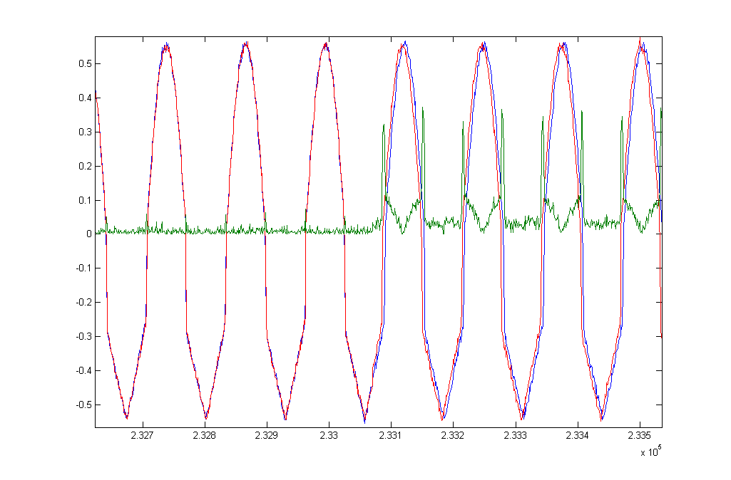
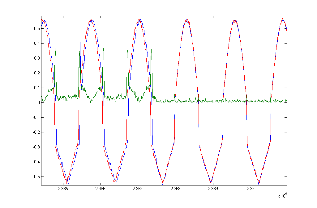
In this another captured picture, both DAC are synchronized, but in some moment, one of the DACs some samples are losing, and signals are desynchronized.After some small random period, some samples are losing in the other DAC, as you can see at this other picture.

I was thinking about it, and I decided to generate 2 ROMS and read with each of DAC clock. At that time, desynchronize problem disappears.

As far as I understand, all of these created clocks couldn't not be the same. I mean, maybe one has 249.99Mhz, and the other one has 250.01 Mhz, and this can produce that FIFO pointers can cross. 

I was looking up some solution for this problem. The best option I found was, reset from time to time, in order to avoid this cross pointers.

I tried this option, but the problem didn't solve.


Do you have any idea that how I can solve this problem?

Thanks

Regards,

Jose Correcher

  • Hi Jose,

    Yes, it seems like the clocks are not synchronized among the different time domains. How are these clocks being generated? Can you draw a diagram of where all of the clocks are coming from and where they're going?

    Note that in our lab testing, we provide a clock from a signal generator to our EVM. On the DAC EVM we have a clock chip, which provides a divided down version back to the FPGA. The divided down clock is used to run the FPGA, including reading from the onboard RAM and outputting to the DAC. In this way, the time domains are all synchronized.

    Regards,
    Matt Guibord 

  • Hi,

    I am only familiar with Altera's serdes, these have a core-clock output which would be derived from the same source as the DCLK to the DAC. I expect Xilinx have something similar. Your FIFO output must be driven from this as the DAC internal buffer is quite small. Can you check the DLL Lock bit? Recent info from TI suggests the DLL can take 100s of microseconds to lock.

    Regards,

    SR

  • Hi Simon,

    As you said, I send DATA, DCLK and SYNC synchronized from FPGA to DAC, by using a SERDES (oserdes) block that Virtex has embedded.

    During DAC configuration, I check that both DAC are locked, and after then I send a test pattern in order to check if there is some error.

    Regards,

    Jose

  • Hi Matt,

    As you can see at this data flow, I generate DAC clocks with AD9517 device, from Analog devices. As far as the ROM clock is concerned, I use the clock system.

    I use different MMCM in order to provide the properly clocks.

    Regards, 

    Jose

  • Hi Jose,

    Thank you for the detailed diagram. Since SysClk and the AD9517 are not synchronized, it is not unexpected to see the shift in data. The easiest way to fix this is to synchronize the SysClk and clock chip. I'm not familiar with the AD9517, but the LMK04800 from TI could be locked to the SysClk using the internal PLL. The other option, and probably easier one, is to use the clock chip to generate the system clock. Can you bring a clock from the AD9517 onto the board as the SysClk?

    Regards,
    Matt Guibord 

  • Hi Matt,

    I solved the problem somedays ago, but I couldn't answer until now.

    Finally I used clk250 from AD9517 and all works properly, thank you!

    Regards,

    Jose Correcher