This thread has been locked.

If you have a related question, please click the "Ask a related question" button in the top right corner. The newly created question will be automatically linked to this question.

Problem with ADS1218

Other Parts Discussed in Thread: ADS1218

Hello, I try to use ADS1218 with MSP430. I want to do conversation of voltage on Ain2 input channel. Without executing SELFCALL cmd, value is not accurate (~0.2 V deviation).

So I tried make SELFCALL, and I understood some terrible thing: every time when i make SELFCALL again (when restart MC) OCR register has different values in range 100 - 4000. First time on DRDY interrupt FSR and ACR registers has 0 values.

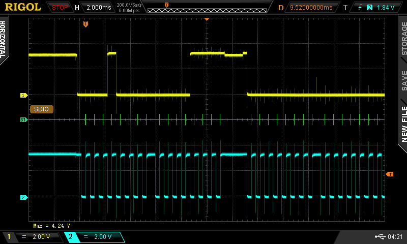
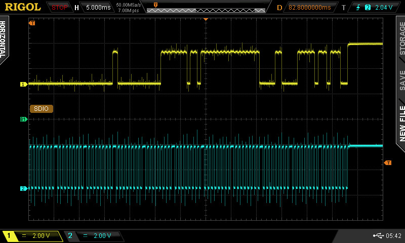
So what I have: F_osc on ADC = 4.9152 MHz, MCLK of MSP430 = 16 MHz, SPI CLK = 32 kHz. I used unipolar mode, max decimation.

This is code. Initialization:

ads1218_init(); //initialize pins and SPI module
__delay_cycles(500000); 

ads1218_send_SELFCAL_command(); //self autocalibrate OFFSET and GAIN

uint8_t data = BIT3; //SPEED=0 - F_mod=F_osc/128, REF EN = 1, REF HI = 0 - Vref = 1.25, BUF EN = 0
ads1218_write_register(ADS1218_SETUP_REGISTER, 0x01, &data);

data = 0x7 + BIT4 + BIT5 + BIT6; // Decimation high 3 bits and sinc3 filtering mode
ads1218_write_register(ADS1218_MDEC1_REGISTER, 0x01, &data);

data = 0xFF ; // Decimation low 8 bits FF
ads1218_write_register(ADS1218_DEC0_REGISTER, 0x01, &data);

ads1218_set_channel(ADS1218_MUXP_AIN2 + ADS1218_MUXN_AINCOM); //select ADS positive and negative channels

/* F_mod=F_osc/128 = 4.9152 MHz / 128 = 38400 Hz
Data Reit = F_mod / dec = 38400 Hz / 2047 = 18.7 Hz; */

P2IE |= BIT7; // P2.7 interrupt enable
SET_BIT(ADC_NOT_DSYNC); //start conversation

And DRDY interrupt:

#pragma vector=PORT2_VECTOR
__interrupt void Port_2(void)
{
  ocr_val = ads1218_read_OCR();
  fsr_val = ads1218_read_FSR(); //when we read here first time ocr_val = 0, and fsr_val =0.

  if (++drdy_div == 4) { // In sinc3 filtering we must skip 3 data convertions
     ads1218_rdata_cmd();
     temp_data = ads1218_read_data();
     uint8_t voltage = temp_data * 1.25 * 100 / 0xFFFFFF; // voltage scalled for 100
     drdy_div = 0;
  }

   P2IFG &= ~BIT7; // clear IFG
}

I attached detailed sources with all used function : 

SPI works perfectly - I tried to read default values of registers, and tried to write/read - all right. 

My questions:

1) what is reason of problem with OCR?

2) where can I find some code examples with using ADS1218 or similar ADC? Please give me some links. I tried searching for it, but I can't find anything on official ADS1218 page.

3)where can I find all time specifications ? ( for example time of the ADC initialization - I am using 500000 ticks of the MCLK, whitout it SPI did not work, In datasheet (SBAS187C) I can't find it, i see there only SPI time specifications.)

Please help. 

  • Hi Van,

    Welcome to the forum!  Let's start with the example code first.  Currently I do not have a complete project ready to post.  I've been working on it, but at this time it is not quite ready as there is a lot to do for this part. 

    As far as your code, it looks to be ok for the most part.  In your interrupt routine you are gathering a lot of information, and I don't think you need to do this.  You should just be running the RDATA command.  I understand that you are trying to evaluate the OCR/FSR settings.  However, the values only change on calibration.  On page 18 of the datasheet it discusses that you should calibrate after power on, a change in decimation or a change in PGA settings.  I see you run the calibration after power on, but not after you change the register settings.  I would move the SELFCAL command to after you set the register values instead of before.  The SELFCAL is actually done taking a number of measurements and averaging them.  In theory the register values should move very little, however due to reference and supply noise the value can move around quite a bit.  Make sure you have a cap on VREFOUT to help keep the reference stable.

    If you short the inputs together to mid-supply you will see how much the code deviates due to noise.  Layout is very critical to achieving great performance.  If the shorted input test shows that you are getting a larger than expected code variation from peak to peak, then the SELFCAL procedure will not be stable and you will see a lot of difference from calibration to calibration.

    The initial startup delay is a factor of many things.  Supply ramp rate, and pin control settings must be in a valid state.  Also, nothing on the device will function until the oscillator clock is running.  If you are using a crystal, you need to see how long it takes for the crystal to start oscillating.  This is more layout/design dependent than part dependent.  If you are driving the control lines (Powerdown, DSYNC, RESET, etc.) from the MSP430 then you must consider the time it takes for these pins to be valid.  The actual RESET time from rising edge of RESET is shown in the Timing Specification Table of the datasheet on page 9.  RESET takes 2640 tosc periods.

    Best regards,

    Bob B

  • Thank you very much for your reply! I apologize for the so long answering. I carried out experimentation with ADC and explored its behavior. Vrcap was unconnected. After adding it, OCR  stabilized from reset to reset (890 - 891). But sometimes it get a strange large values such as 49345.

    Now scheme is:

    And I want to measure 1.3 Volt on In pin.

    I changed main code to:

    ads1218_init(); //initialize pins and SPI module
    __delay_cycles(5000000);

    uint8_t data = REF_EN + REF_HI + BUF_EN; // SPEED=0 - F_mod=F_osc/128, REF EN = 1, REF HI = 0 - Vref = 2.5, BUF EN 

    ads1218_write_register(ADS1218_SETUP_REGISTER, 0x01, &data);

    data = 0x7 + SINC3 + UNIPOLAR; // Decimation high 3 bits and sinc3 filtering mode + Unipolar + BIT4 + BIT5 + BIT6
    ads1218_write_register(ADS1218_MDEC1_REGISTER, 0x01, &data);

    data = 0xFF ; // Decimation low 8 bits FF
    ads1218_write_register(ADS1218_DEC0_REGISTER, 0x01, &data);

    ads1218_send_SELFCAL_command(); //self autocalibrate OFFSET and GAIN

    ads1218_set_channel(ADS1218_MUXP_AIN4 + ADS1218_MUXN_AINCOM); //select ADS positive and negative channels

    /* F_mod=F_osc/128 = 4.9152 MHz / 128 = 38400 Hz
    Data Reit = F_mod / dec = 38400 Hz / 2047 = 18.7 Hz; */
    P2IE |= BIT7; // P2.7 interrupt enable
    __delay_cycles(16);
    SET_BIT(ADC_NOT_DSYNC); //start conversion
    }

    #pragma vector=PORT2_VECTOR
    __interrupt void Port_2(void)
    {
      if (++drdy_div == 4) { // In sinc3 filtering we must skip 3 data convertions
         ads1218_rdata_cmd();
         temp_data = ads1218_read_data();
         volatile float f_voltage = temp_data * 2.5 / 0x1000000;

         drdy_div = 0;
      }
      P2IFG &= ~BIT7; // clear IFG
    }

    Now on first reading f_voltage = 1.25, and on other readings temp_data = 0; When I connect In to AGND it behaves in the same.When I comment the callibration, values on each reading have is very different. 

    Regards, Ivan

  • Hi Ivan,

    I cannot see anything obviously wrong with your code or procedure.  If you are running the debugger, sometimes things can messed up in interrupt routines if you are setting a breakpoint in the routine.

    I would monitor DOUT/SCLK with a scope to see if the output is really zero.  This will narrow the problem to either the ADS1218 configuration, or software.

    Another point I should make is that once you have settled data you do not need to wait 3 conversion cycles unless there is a stepped change or a mux change.  This is because each settled result only depends on the current result plus the previous two.

    Best regards,

    Bob B

  • Hello everybody,

    I noticed this conversation and since i am having a similar problem, i will continue here...

    I am also testing the ADS1218, trying to measure the voltage on the internal diode. I set the idac1 current to 35uA and measure the voltage (i am sure the current is set because i can measure it on external idac1 pin.).  I set the mux to 0xff. But what i am getting is same strange value which is fixed and not even the last bits are changing.

    Then i started to analyze the sefcal results, and i can see they are not even close to be similar one to another selfcal procedure (please see below). Every selfcal procedure returns a completely different result. I  have a cap on VREFOUT pin. I have no idea what else could be the problem. Can you please give me some hint what could be wrong?

    Best Regards

    Klemen

    # ./selfCal.py
    # ./readReg.py
    Reg  0x00: SETUP  0x4a
    Reg  0X01: MUX    0x1
    Reg  0X02: ACR    0x18
    Reg  0X03: IDAC1  0x2
    Reg  0X04: IDAC2  0x0
    Reg  0X05: ODAC   0x0
    Reg  0X06: DIO    0x0
    Reg  0X07: DIR    0x0
    Reg  0X08: DEC0   0x80
    Reg  0X09: M/DEC1 0x7
    Reg  0X0A: OCR0   0xad
    Reg  0X0B: OCR1   0x37
    Reg  0X0C: OCR2   0xf2
    Reg  0X0D: FSR0   0xf0
    Reg  0X0E: FSR1   0xa6
    Reg  0X0F: FSR2   0x61
    # ./selfCal.py
    # ./readReg.py
    Reg  0x00: SETUP  0x4a
    Reg  0X01: MUX    0x1
    Reg  0X02: ACR    0x18
    Reg  0X03: IDAC1  0x2
    Reg  0X04: IDAC2  0x0
    Reg  0X05: ODAC   0x0
    Reg  0X06: DIO    0x0
    Reg  0X07: DIR    0x0
    Reg  0X08: DEC0   0x80
    Reg  0X09: M/DEC1 0x7
    Reg  0X0A: OCR0   0x2f
    Reg  0X0B: OCR1   0xda
    Reg  0X0C: OCR2   0xf1
    Reg  0X0D: FSR0   0x6b
    Reg  0X0E: FSR1   0x27
    Reg  0X0F: FSR2   0x6a
    # ./selfCal.py
    # ./readReg.py
    Reg  0x00: SETUP  0x4a
    Reg  0X01: MUX    0x1
    Reg  0X02: ACR    0x18
    Reg  0X03: IDAC1  0x2
    Reg  0X04: IDAC2  0x0
    Reg  0X05: ODAC   0x0
    Reg  0X06: DIO    0x0
    Reg  0X07: DIR    0x0
    Reg  0X08: DEC0   0x80
    Reg  0X09: M/DEC1 0x7
    Reg  0X0A: OCR0   0x58
    Reg  0X0B: OCR1   0xfb
    Reg  0X0C: OCR2   0xff
    Reg  0X0D: FSR0   0x7
    Reg  0X0E: FSR1   0x0
    Reg  0X0F: FSR2   0x90

  • Hi Klemen,

    Welcome to the forum! The SELFCAL does require a stable reference.  What are the register settings you are using prior to SELFCAL?  Can you send me your schematic, PCB layout, and scope shots of the communication?

    Thanks,

    Bob B

  • Thank you for your reply,

    All the register settings can be seen from the register printout i pasted above: internal reference is enabled and set to 1.25 V.

    I connected Vref- to Gnd and Vref+ to Vrefout. I have 1000 pF ceramic capacitor on Vrcap pin and two 100nF on Vrefout pin. I can make a photo of my pcb if you think this will help?

    I measured the Vref+ voltage with the oscilloscope (HP 54600A) and it showed 1.249 V avg / 25 mV p-p.

    I can send you a scopeshot of communication - but can you be more specific which one? I think the communication is OK because i can read and write to registers and the values i read match the values i write.

    Best Regards

    Klemen

  • Hi Klemen,

    Please send me a scope shots of CS, SCLK, DIN and DOUT for register write and register read.

    Best regards,

    Bob B

  • My readout

    ./readReg.py
    Reg  0x00: SETUP  0x4a
    Reg  0X01: MUX    0x1
    Reg  0X02: ACR    0x0
    Reg  0X03: IDAC1  0x0
    Reg  0X04: IDAC2  0x0
    Reg  0X05: ODAC   0x0
    Reg  0X06: DIO    0x0
    Reg  0X07: DIR    0x0
    Reg  0X08: DEC0   0x80
    Reg  0X09: M/DEC1 0x7
    Reg  0X0A: OCR0   0xf6
    Reg  0X0B: OCR1   0xff
    Reg  0X0C: OCR2   0xff
    Reg  0X0D: FSR0   0xc
    Reg  0X0E: FSR1   0x3e
    Reg  0X0F: FSR2   0xdc

    Scope: Clk, Dout

    Scope: Clk, Din

    Zoom in - first part

    Zoom in - second part

  • Hi Klemen,

    Thanks for the scope shots.  The Dout seems to be ok, but I do have concerns about the data coming into the ADS1218.  Notice how the Din appears to drop in voltage level when clocking starts.  I don't believe that the logic high is even a valid logic level for the device (0.8*DVDD).

    I think you may have some connections issues.  You should not see the voltage level drop on the communication.  Also, based on the calibration registers it would seem there are some issues with the reference connection too.  This might also be caused by a poor/inadequate ground.

    Are you using a proto type board, or an actual PCB?  Can you send me your schematic and layout?

    Best regards,

    Bob B

  • Thank you for your reply,

    The ads1218 is soldered on pcb and the communication and power supply lines are wired through the protoboard to BeagleBone black which is used for the communication.

    I made a photo of the pcb (i don't have the schematics since there are just few components on the pcb). The ground is joined below the ads1218. The three 1206 capacitors right to ads1218 are 100 nF and one 1206 capacitor left to ads1218 is 1000 pF. The Vref+ and Vref- lines are joined to Vrefout and Gnd using two jumpers (the pads can be seen just above the capacitors). I hope this explains the layout clearly enough.

    Best Regards,

    Klemen

  • Hi Klemen,

    You have a very well organized layout, but it is inadequate for high levels of 24-bit performance. To get a better idea regarding what I'm talking about please see the layout information on the E2E wiki:

    http://e2e.ti.com/support/data_converters/precision_data_converters/w/design_notes/grounding-techniques.aspx

    Primarily you need to be concerned about return currents.  I'm also a bit surprised the crystal starts.  Often times the small trace for the cap ground is insufficient to start oscillation.  I would suggest adding more ground area on the opposite side of the board to create a plane.  Also widen the digital ground trace to reduce inductance.

    One thing that is not clear to me is the reference connections.  I assume they connect to the caps, and also to the jumpers.  I don't see where the VREFOUT connects.  Is it directly connected under the center cap?  The trace appears to just end between the center and rightmost cap.

    Best regards,

    Bob B

  • Thank you for your reply,

    The traces you marked make a 90 degree turn up below the cap and are wired together with a jumper on the other side of the board. I see now that a didn't put enough effort into a pcb design. I will make a new one - i will let you know if that solved my problem :) Thank you very much for your help and your time!

    Regards

    Klemen

  • Hi Van Bor,

    Have you got ADS1218 working on TIVA processor, Can you please forward that code if possible as I am struggling to get SPI based ADS1218 working on TIVA processor using TIVA peripheral library. It would be a great help if you can forward your ADS1218 working code(complete project).

    Eagerly waiting for your response as I am not able to get ADS1218 working sample code on web.

    Regards,

    Mritunjai

  • Hi Van, I am also trying to use ADS1218 with MSP430. However, I nearly can't find any code example for ADS1218. Can you send me the code for ADS1218 if it is convenient for you. Thank you very much. My email is wt20094324@163.com