This thread has been locked.

If you have a related question, please click the "Ask a related question" button in the top right corner. The newly created question will be automatically linked to this question.

Question about the Application about 16-Bit ADC "ADS1148"

Other Parts Discussed in Thread: ADS1148

I have read the datasheet of "ADS1148" and there are 7 Single-Ended Inputs on the "ADS1148", but there is no application circuit example  for the Single-Ended Inputs on the datasheet.

There are too many pins on "ADS1148" and I am not sure how to use them.

I want to measure 7 analogsignals and the area of analogsignal is 0 to 10V.

Can you give me a application circuit for 7 Single-Ended Inputs?

I look forward to your answer.

  • Lidong,

    The basic single ended measurement is based on a signal referenced to ground.  In other words, 0V is 0 potential as measured from the reference point of ground.  So to get 7 single ended measurements, you need to set one input to ground (for example AIN7 should have the mux connection to AINN) and the other inputs connect then to AIN0-AIN6 to AINP.

    But you have a couple of problems.  10V exceeds the absolute maximum input voltage, so this needs to be reduced.  One way to do this is with a voltage divider.  Your voltage divider needs to be relative to the reference voltage that produces a positive full scale input.  Using the internal reference with a gain of 1, this is 2.048V.

    The other issue is the common mode restriction of the PGA.  The only way you can get a measurement to ground (0V) is to use a bipolar supply.  See this Design Notes page for further information:

    http://e2e.ti.com/support/data_converters/precision_data_converters/w/design_notes/1370.input-voltage-range-requirements-for-the-ads1248-and-ads1148-families.aspx

    Best regards,

    Bob B

  • Thank your very much for your answer!

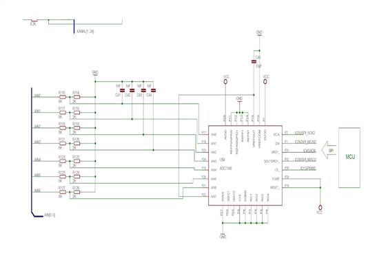
    I have drawed a circuit and I have chosen the "voltage divider " for 7 analog signal(0-10V).

    I have a MCU with SPI interface to control the ADS1148, VCC is 3.3V. Can you give me some suggestion about the circuit, whether the circuit has the right connection?

  • Lidong,

    Please review the link I sent before.  You cannot make single ended measurements with a unipolar supply with the ADS1148.  You also need bypass caps, and there needs to be a cap across VREFOUT and VREFCOM, and VREFCOM should be connected to ground.  The internal reference is limited to 2.048 volts, so the input voltage divider must be calculated to stay within that range.

    Best regards,

    Bob B

  • Hello Bob,

    How can I initialize ADS1148, choose one channel by one channel of ADS1148 and read the analog-input value? I use "EMX Module"of GHI to controll the ADS1148. We have disscussed the schematic of ADS1148 last year.

    The schematic is in the last posts. I use Single-Ended Input to measure the 6 Analog-input-signal(0...10V), AIN7 is to GND. I have used a voltage divider to reduce the input-volt(max.2V).

    I have written a example code as follow to controll the AIN0 of ADS1148.

            static InputPort    DRDY_   = new InputPort((Cpu.Pin)EMX.Pin.IO33, false, Port.ResistorMode.PullUp);
            static OutputPort START    = new OutputPort((Cpu.Pin)EMX.Pin.IO37, true);
            static OutputPort RESET_ =  new OutputPort((Cpu.Pin)EMX.Pin.IO32, true);


            static byte[] WREG    =  new byte[6] { 0x44, 0x03, 0x07, 0x01, 0x00, 0x0F}; //initil ADS1148 Register "MUX0", "VBIAS", "MUX1", "SYS0"
            static byte[] TX_NOP  =  new byte[2] { 0xFF, 0xFF }; // NOP bytes for SPI-writing
            static byte[] RX_NOP  =  new byte[2]; // NOP bytes for SPI-reading

    main()

    {

           ..................................................

            ........................................................

                Thread Analog_input = new Thread(Analog_input_Thread_Loop);
                Analog_input.Start();

    }

            static void Analog_input_Thread_Loop() //20ms
            {

                while (true)
                               {

                                          START.Write(true);   //start Logic HIGH

                                          RESET_.Write(true);//reset Logic HIGH

                                           SPI_1.Write(WREG); // send WREG to initialize ADS1148 Register "MUX0", "VBIAS", "MUX1", "SYS0"

                                           SPI_1.WriteRead(TX_NOP,RX_NOP); //Send NOP and read DOUT

                                            AIN0 = RX_NOP[0] * 256 + RX_NOP[1]; // Covert the 16bit SPI MISO Siginal to a int                                      

                                           AIN0_String = AIN0.ToString("N1");// convert int to string
                        
                                            Thread.Sleep(20);

                                }

             }

    but it doesn'ts work, I always got the "0" value of AIN0. what is the problem of my codes? where is wrong? Can you give me some suggestion?

    I look forward to your answer!

  • Lidong,

    I hope you made the changes to your schematic that I mentioned before.  Start and Reset pin needs to be logic high.  There must be a cap across VREFCOM and VREFOUT.  VREFCOM should connect to ground.

    This command is wrong:

    static byte[] WREG    =  new byte[6] { 0x44, 0x03, 0x07, 0x01, 0x00, 0x0F}; //initil ADS1148 Register "MUX0", "VBIAS", "MUX1", "SYS0"

    and should be:

    static byte[] WREG    =  new byte[6] { 0x40, 0x03, 0x07, 0x01, 0x30, 0x0F}; //initil ADS1148 Register "MUX0", "VBIAS", "MUX1", "SYS0"

    You need to verify that your communication is correct with an oscilloscope.

    Best regards,

    Bob B

  • I have changed the schematic as follow:

    I need 4 channels(AIN0,1,2,3) as my analoginputs, AIN7 is to GND. the RESET_ and START are to VCC(3.3V).

    How can I choose the Channel one by one in a loop? I want to read my 4 Analoginputs one by one continously. I have written somes codes as follow, can you give me some suggestion?

    main()

    {

                int channel=0;

                //initialize ADS1148, AN0 is chosen,

                byte[] WREG    =  new byte[6] { 0x40, 0x03, 0x07, 0x01, 0x30, 0x0F}; //initil ADS1148 Register "MUX0", "VBIAS", "MUX1", "SYS0" 

             byte[] RDATA    =  new byte[1] {0x12};

    byte[] NOP    =  new byte[1] {0xFF};

                // send WREG to initialize ADS1148 Register "MUX0", "VBIAS", "MUX1", "SYS0

                SPI.Write(WREG); 


                //defeine a thread 10ms

                Thread Analog_input = new Thread(Analog_input_Thread_Loop);
                Analog_input.Start();

    }

            static void Analog_input_Thread_Loop() //10ms
            {

                while (true)
                               {

                                    if(channel==0)

                                    {

                                          //choose AIN0 channel, AIN0 is positiv and AIN7 is negativ

                                          byte[] WREG    =  new byte[4] { 0x40, 0x01, 0x07, 0x01};

                                          SPI.Write(WREG);

                                          SPI.Write(RDATA);

                                          Data_MSB = SPI.Read(NOP);

                                          Data_LSB  = SPI.Read(NOP);

                                          Data = 256*Data_MSB + Data_LSB;

                                    }

                                    else if(channel==1)

                                    {   

                                         //choose AIN1 channel, AIN1 is positiv and AIN7 is negativ

                                          byte[] WREG    =  new byte[4] { 0x40, 0x01, 0x0F, 0x02};

                                          SPI.Write(WREG);

                                          SPI.Write(RDATA);

                                          Data_MSB = SPI.Read(NOP);

                                          Data_LSB  = SPI.Read(NOP);

                                          Data = 256*Data_MSB + Data_LSB;

                                    }

                                    else if(channel==2)

                                    {

                                          //choose AIN2 channel, AIN2 is positiv and AIN7 is negativ

                                          byte[] WREG    =  new byte[4] { 0x40, 0x01, 0x17, 0x04};

                                          SPI.Write(WREG);

                                          SPI.Write(RDATA);

                                          Data_MSB = SPI.Read(NOP);

                                          Data_LSB  = SPI.Read(NOP);

                                          Data = 256*Data_MSB + Data_LSB;

                                    }

                                    else if(channel==3)

                                    {     

                                         //choose AIN3 channel, AIN3 is positiv and AIN7 is negativ

                                          byte[] WREG    =  new byte[4] { 0x40, 0x01, 0x1F, 0x08};

                                          SPI.Write(WREG);

                                          SPI.Write(RDATA);

                                          Data_MSB = SPI.Read(NOP);

                                          Data_LSB  = SPI.Read(NOP);

                                          Data = 256*Data_MSB + Data_LSB;

                                    }

                                    channel++;

                                  if(channel ==4) channel=0;

                                  Thread.Sleep(10);

                               }

             }

  • Lidong,

    That is the basic flow, but you need to know when the data is valid.  You need to monitor DRDY either by polling or by interrupt to know when it transitions low signaling valid data.

    Also, you are still not understanding the concept of measuring within the common mode range of the device.  AIN- cannot be connected to ground when using AVSS connected to ground.

    Best regards,

    Bob B

  • thank you very much, you are right! I forgot the Pin "DRDY", I should check it to kown the transition's situation.

    I am confused about the schematic, how can I connect the input signal to ADC1148?

    You told me in the post of Dec 03 2012 20:22 PM as follow

    "you need to set one input to ground (for example AIN7 should have the mux connection to AINN) and the other inputs connect then to AIN0-AIN6 to AINP."

    sorry that I have too little experience about "ADS1148", how can I connect AIN(0....7) to AIN(N/P)? there are no AINN and AINP pins in ADS1148.

    have drawn the schematic again, I used Single-Ended Inputs to measure analoginpus(0...10V), I have used voltage divider to reduce the inputvolt to maximal 2.048V

    If AIN- cannot be connected to ground when using AVSS connected to ground, how can I connect my analoginputs to ADS1148? I look forward to your answer.

    best regards

    Lidong


  • Lidong,

    From the same post you cited I also stated the following:

    The other issue is the common mode restriction of the PGA.  The only way you can get a measurement to ground (0V) is to use a bipolar supply.  See this Design Notes page for further information:

    http://e2e.ti.com/support/data_converters/precision_data_converters/w/design_notes/1370.input-voltage-range-requirements-for-the-ads1248-and-ads1148-families.aspx

    If you take a look at Figure 51 of the datasheet you will notice that the mux can be switched in a variety of ways.  The input to the PGA is shown as a differntial input of AINP and AINN.  This means that for a positive value for the output code the relative value of P is greater than N.  For the MUX0 register settings, the P (positive input channel) corresponds to MUX_SP, and the N (negative input channel) corresponds to MUX_SN.

    One possibility for attempting to read single ended inputs for a unipolar supply (AVSS connected to ground) is to bias the analog input for AIN7 to a value above ground.  For example, you could connect AIN7 to VREFOUT.  Now the differential measurement will be different as at 2.048V (with AIN0 equal to 2.048V and the AIN7 also at 2.048V for example) the differential resultant code will be zero.  In this case you need to make a calculation where  you subtract the output code from the full scale code value to achieve the correct value.  2.048V - 0V = 2.048V is the example we just used.  In hex you would use 0x7ff - 0x0000 = 0x7fff.

    There is one problem, and that is when your input is below 0.1V as this places you outside the common mode range of the ADS1148 (assuming a PGA gain of 1.)  However, in most cases that should work out ok if your signal is mostly above 0.1V.

    Best regards,

    Bob B

  • hello Bob,

    thank you for your help! I have changed schematic and tried ADS1148 again. Actually I need only 4 Inputs for my project, I give the 4 inpus(AIN0 to AIN3) the same signals (about 0.5 to 2V after voltage divider), the signals are from the same voltage source.

    I got the different values from from AIN0 to AIN3, why?

    for example:

    if Analoginput is 0.644V, I got the digits as follow:

    A0: 25071
    A1: 25076
    A2: 25616
    A3: 25720

    if Analoginput is 1.066V, I got the digits as follow:

    AIN0: 26752
    AIN1: 26785
    AIN2: 27041
    AIN3: 27086

    if Analoginput is 1.303V, I got the digits as follow:

    AIN0: 27702
    AIN1: 27723
    AIN2: 27838
    AIN3: 27865

    if Analoginput is 1.622V, I got the digits as follow:

    AIN0: 28949
    AIN1: 28943
    AIN2: 28871
    AIN3: 28879

    I find, if volt of input is small, the difference of digits are big.

    I read the the data continuously. I initialize the registers again, after changing MUX channel.

    The thread task for ADS1148 is as follow:

            static byte[] WREG_0 = new byte[6] { 0x40, 0x03, 0x07, 0x01, 0x30, 0x0F};
            static byte[] WREG_1 = new byte[6] { 0x40, 0x03, 0x0F, 0x02, 0x30, 0x0F};
            static byte[] WREG_2 = new byte[6] { 0x40, 0x03, 0x17, 0x04, 0x30, 0x0F};
            static byte[] WREG_3 = new byte[6] { 0x40, 0x03, 0x1F, 0x08, 0x30, 0x0F};
            static byte[] WREG_4 = new byte[6] { 0x40, 0x03, 0x27, 0x10, 0x30, 0x0F};
            static byte[] WREG_5 = new byte[6] { 0x40, 0x03, 0x2F, 0x20, 0x30, 0x0F};
            static byte[] WREG_6 = new byte[6] { 0x40, 0x03, 0x37, 0x40, 0x30, 0x0F};
            static byte[] RDATA  = new byte[1] { 0x12};
            static byte[] RDATAC = new byte[1] { 0x14};
            static byte[] SDATAC = new byte[1] { 0x16};
            static byte[] WAKEUP = new byte[1] { 0x00};

            static byte[] TX_NOP_16bit    = new byte[2] { 0xFF, 0xFF };
            static byte[] RX_NOP_16bit_0 = new byte[2];
            static byte[] RX_NOP_16bit_1 = new byte[2];
            static byte[] RX_NOP_16bit_2 = new byte[2];
            static byte[] RX_NOP_16bit_3 = new byte[2];

     static void AnaloginputLoop()
            {
                while (true)
                {
                    if (initail_ready == false)
                    {
                        if (channel == 0) SPI_2.Write(WREG_0);
                        if (channel == 1) SPI_2.Write(WREG_1);
                        if (channel == 2) SPI_2.Write(WREG_2);
                        if (channel == 3) SPI_2.Write(WREG_3);
                        SPI_2.Write(WAKEUP);
                        SPI_2.Write(RDATAC);
                        initail_ready = true;
                    }

                    if (DRDY_.Read() == false)
                    {
                                           
                        if (channel == 0)
                        {
                            SPI_2.WriteRead(TX_NOP_16bit, RX_NOP_16bit_0);
                            result_0 = 256 * RX_NOP_16bit_0[0] + RX_NOP_16bit_0[1];
                            A0_String = result_0.ToString();
                            initail_readdy = false;
                        }

                        if (channel == 1)
                        {
                            SPI_2.WriteRead(TX_NOP_16bit, RX_NOP_16bit_1);
                            result_1 = 256 * RX_NOP_16bit_1[0] + RX_NOP_16bit_1[1];
                            A1_String = result_1.ToString();
                            initail_ready = false;
                        }

                        if (channel == 2)
                        {
                            SPI_2.WriteRead(TX_NOP_16bit, RX_NOP_16bit_2);
                            result_2 = 256 * RX_NOP_16bit_2[0] + RX_NOP_16bit_2[1];
                            A2_String = result_2.ToString();
                            initail_ready = false;
                        }

                        if (channel == 3)
                        {
                            SPI_2.WriteRead(TX_NOP_16bit, RX_NOP_16bit_3);
                            result_3 = 256 * RX_NOP_16bit_3[0] + RX_NOP_16bit_3[1];
                            A3_String = result_3.ToString();
                            initail_ready = false;
                        }
                       
                        channel++;
                        if (channel == 4) channel = 0;

                    }

                    Thread.Sleep(10);
                }
            }

    the schematic is as follow:

    Can you give me some suggestion? or Is there somethingswrong in my schematic and thread task?

    I look forward to your answer!

    best regards

    Lidong

  • Lidong,

    I see you have VBIAS turned on for each measurement.  Keep VBIAS at 0x00, as this voltage will create a problem by creating an additional current path, especially at the lower voltage inputs.

    It is not totally clear if you are applying the input voltages described directly to the ADC input, or through the voltage divider.  If you are placing the input through the voltage divider, the resistors need to be very well matched or the variance in the resistor tolerance will alter the result accordingly.  Another issue is you are setting the data rate to 2000sps.  This will have some code variation due to noise.  Another possibility is the stability of the voltage source.  If the source is noisy, you will see code variation from reading to reading.

    As you also have a filter at the input, you need to wait for the analog inputs to fully settle before making the measurements.

    There also appears to be a calculation issue with respect to the codes you are using.  With a 2.048 voltage reference, the LSB size is about 62.5uV.  If I assume that you are applying 0.644V directly to the analog input of the ADS1148, that should result in a code relative to ground of about 10304 (0.644/62.5uV.)  However, the resultant code is not referenced to ground, but to 2.048V.  This means you should get a negative output code.  The actual input should result in a difference of -1.404V.  This should be -22464 codes.  Positive full-scale is 32767 codes.  If you take full scale and add the difference (32767 + (-22464)) you should get the value relative to ground, which is 10304.  The result you are getting is much different.  Here you have to be careful that you maintain the correct sign.  If you use a signed short for your data result you should be ok, but if you use a signed int, then you need to sign extend appropriately.

    The calculation of the result should be the total counts times the LSB size.  This value will be greater than 32767 for all input voltages greater than 2.048V and less than 32767 for all voltages less than 2.048V.

    First thing to do is make sure VBIAS is off.  You should then verify your computed data with results by monitoring DOUT with an oscilloscope.  They should match by both computed and hand calculation.

    Best regards,

    Bob B