This thread has been locked.

If you have a related question, please click the "Ask a related question" button in the top right corner. The newly created question will be automatically linked to this question.

ADS8327 how to get the data via SPI

Genius 4170 points
Other Parts Discussed in Thread: ADS8327, MSP430F5437A

Hello,

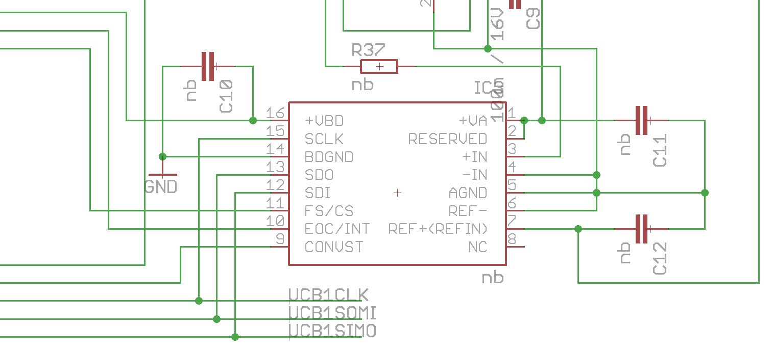
I want to use my MSP430F5437A with an external ADC, therefore I chose the ADS8327 16-bit type, and until now I couldnt find out a easy to understand way to get the data out of this ADC into my MSP430. To be honset I just did start reading the manual and making my first moves on this particular ADC. I am pretty fluent with the MSP430 and C programming, so I have no doubts I will accomplish to read it out someday, but the faster the better.

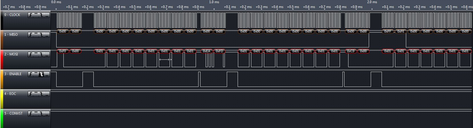
What I did expect to find in the datasheet is some kind of commands, that I could send via SPI and get a response with the 16 bit results afterwards from the ADC. I did already program an external SPI Flash device which was pretty straight forward and easy to understand, but unfortunatly the ADC is not that easy.

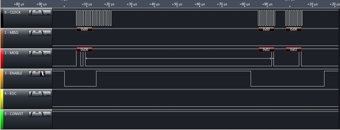
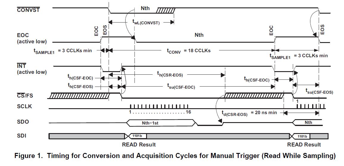
There are some nice figures on page  13 with using the device in manual trigger mode, I think my next step will be to try managing my commands around this figure, although I am confused where I do get my conversion result back? and with what timing.

So if anyone in  here already did work with this ADC and wants to share their experiencce with me I really would appreciate this.

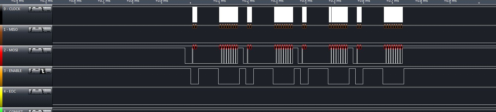
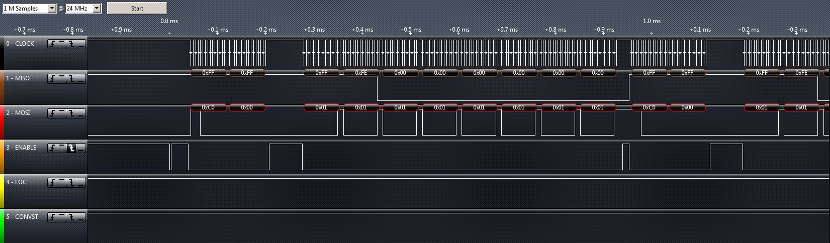
I keep this post updated whenever I achieve some goals with the ADC for myselfe, as long as someone seems interested or even responds :D

Greets and thanks for reading,

Seb

  • Hello Seb,

    The ADS8327 SAR converter can support up to 500kHz sampling rate.   The clock used for conversion may be internal or external, in other words, the SCLK may be used as an I/O clock only or as I/O clock and conversion clock.  When using the external SCLK to control the conversions, the SCLK is reduced to half of its frequency before it is used for a conversion clock (CCLK). 

    The ~CNVST may be used to trigger the conversions in the manual trigger mode, or the conversions may be automatically trigerred if it is programmed (CFR_D9 = 0). When the converter is configured as auto trigger, the next conversion is automatically started three conversion clocks (CCLKs) after the end of a conversion. Page 23-24 of the datasheet provides a detailed explanation about how to control the conversions. 

    The minimum sampling time is 3 CCLKs and the required conversion time is 18 CCLKs. The EOC (end of aquisition or sampling instance) may be used to monitor when a conversion is in progress.  The conversion result is available to the input of the output data register (ODR) at EOC and available at the ODR register at the next falling edge of CS or FS.  For example, on manual mode, the READ command is issued as shown on FIG 1 and the corresponding data is read on the next falling edge of CS/FS.  There are a few ways to configure the device, so please let me know if you have more details about your application requirements.

    Thank you and Best Regards,

    Luis

  • Hello,

    thanks for Your long answer, I kind of feel reminded at the datasheet though.

    So to get back into the practical thing, I will tell You what I just tried. I wanted to start reading out the CFR ( settings ?! ) register of the ADC, as this should be one of simplest things.

    I figured I only have to switch CS to low then transfer the command ( 1100 0000 0000 0000b) to theADC I do that in follwing manner:

    P8.4 is my CS pin coming from the MSP430:


        P8DIR |= BIT4;
        P8OUT &= ~BIT4;

        while (!(UCB1IFG & UCTXIFG));        //Sendepuffer bereit?
        UCB1TXBUF = 0xD0;                    // Read CFR - 1100b
        while (!(UCB1IFG & UCTXIFG));        //Sendepuffer bereit?
        UCB1TXBUF = 0;                    // 8 Dont care bits übertragen

        P8OUT |= BIT4;
        __delay_cycles(100);               I got this delay to just provide some space for the code between the CS signals

    Now with the follwing CS selection the ADC should transfer data via its SDO into my MSP430:

        P8OUT &= ~BIT4;

        while(ByteAnzahl)
        {
            UCB1TXBUF = 2;                        // Dummywrite um Daten zu empfangen
            while (!(UCB1IFG & UCRXIFG));        //Empfangspuffer bereit?
            *Temp_MessungRAM = UCB1RXBUF;                    //Steuerungsdaten senden
            __no_operation();
            Temp_MessungRAM++;                                //Pointer auf daten incementieren
            ByteAnzahl--;
        }
        while(UCB1STAT&UCBUSY);            // BUSY while TX or RX


        P8OUT |= BIT4;

    Now the result of the CFR register sent by the ADC should be present in the address of the pointer  *Temp_MessungRAM

    but there is always 0 right now, which is wrong, so I know the data transfer is not working right now.

    As I said I will keep this up to date until I reach my goal :)

    Thanks for helping

  • Ok first my faults :)

    I did not start the ADC by applying 3,3V to VB, now with that functioning it should work, give me some time.

  • Ok now I can Send data via my MSP430 over the lines, but I am not sure if the ADC gets it???

    Now this is the real question, I was looking to ask from the beginning:

    How do you set up the real practical part ? what do I have to send with what timing in order to get an result.

    As you can see I am transimtting 1100b filles with 0000 and  0000 0000 to send 16 bit into the ADC, then toggling the CS line another time and with the next CS selection I would love to get some data back from the ADC, but it doesnt seem to respond to me, ... yet

    With SPI I always have to send something in order to get something back, so I do send the 2, which gets also transfered but there is simply nothing from the ADC, what could I be doing wrong???

    UPADTE#1:

    I did send the wrong command, it wasnt 0xD0 but 0xC0, I was really happy to see that, but then I tried it with the same frustrating result, no output from the ADC...

  • Hi seb,

    Here are my two cents for the moment.

    Since this part has two ground pins, are the grounds tied together? It could be damaged/malfunction if the two ground pins are or were isolated.

    Thank you,
    Rafael

  • Thanks for your thoughts.

    As I see it there is the analog GND and another one, and indeed I did seperate the flows of those two, but generally they are brought to the same level in one certain point in my PCB layout, so both are on the same voltage level.

    My guess right now is that I am still doing something wrong in demanding the ADC to send me data. This is always the tricky part, I did this once before for an external Flash from Atmel, and it did work pretty straight forward with some minor disturbances :) as every engineer knows. But this ADC's datasheet really is somehow stupid to read, there is not exactly one flow diagram on when to send what command via SPI in roder to achivee something on that stupid ADC...

    Waiting for support till tomorrow :)

    Good night.

  • Hello Seb,

    Please verify your SCLK polarity and phase.  The device accepts CPOL=0, CPHA=1 or CPOL=1, CPHA=0.   The posted scope shot appears to show  POL=1, PHA=1.

    After issuing  0xC000 (READ CFR 16 SCLKs) you should be able to read the default RESET value of ADS8327 which is 0xEFFD 0xEFD (12 bit config register); where CS/FS needs to be held low during the complete 16 SCLK  transaction. The easiest thing to do may be to set up the device in the default manual trigger mode and trigger the conversions using CONVST.  If Schematics are available, please post them as well, these are always helpful so I may understand the set up.

    Best Regards,

    Luis

  • Hello,

    I have been tripping about that field before, while trying to command the Atmel flahs, for some reasons industry didnt find a standart for this polaritiy and phase settings. Since I didnt find a logic clue to solving that riddle I simply tried all settings, and so I did this time, unfortunatly with no results yet:

            UCB1CTL1 |= UCSWRST;                          // **Put state machine in reset**


            //UCB1CTL0 |= UCMST + UCSYNC + UCCKPH + UCMSB; 
            //UCB1CTL0 |= UCMST + UCSYNC + UCCKPH + UCCKPL + UCMSB; 
            //UCB1CTL0 |= UCMST + UCSYNC + UCMSB;             
            UCB1CTL0 |= UCMST + UCSYNC + UCCKPL + UCMSB;        /


            UCB1CTL1 &= ~UCSWRST;                          // **Initialize USCI state machine**

            extADC_test();
            _NOP();

    With following results:

    The important thing on that picture is, that there is no answer from the ADC, and in that picture you can see I send 4 times the read settings out command and wait for the answer with all 4 possible SPI settings CPH and CPOL.

    Any further suggestions?

    Perhaps my 15 € ADC really already broke down, that would be kind of sad, especially because the time I need right now really is growing :)

    PS: here is the basic schematic, I did really cut it down, since I dont want anyone to copy my highly secret thoughts.

    The elements signed with nb are soldered in, in my opinion the electric flow should work, or there is nothing that speaks against it.

  • Hi Seb,

    The code shown on the post above appears to show that you have set up the correct polarity and phase (CPOL=1 and PHA=0); although I am not able to see the detail on the zoomed out scope shot.  To read the CFG register, the transaction needs to be 16 sclk's long holding FS/CS low; where the first 4 bits correspond to the command followed by zero's (Read CFR xC00h).  The SDO should give the CFR value read back, which contains the first four MSBs of conversion data plus the 12 bit CFR register values.   

    The partial schematic only shows the SDO, SDI and SCLK signals. Assuming the AGND, BDGND are at the same potential, and VA, VBD supplies are connected to the appropiate supply rail as described on your previous posts, you should be able to read the register values.  If you already have verified all the voltages and connections, it is possible that the device was damaged. 

    Best Regards,

    Luis  

  • Hello again,

    new week, new ideas.

    Ok most of the errors I did for myself, I do drive my whole application via 3 CR2032 Lithium batteries, they are capable of driving some currents, but I sadly had to find out that the ADC draws some 100 mA in my design ( I did unplug the batteries and put a voltage source on instead, because I spidersensed my power problem after a while ).

    Here comes the next question. Is the current drawn too much, is it becasue of some errors I made while commanding the MSP430 output pins or some PCB failure on the ADC device? ( the traces and solder pads were or are present on all my functioning devices which are already in production and working )

    The datasheet states: 6 mA max current for the ADS8327, I do not have a lot expirience with external ADCs, one collegue said it could be perfectly normal that is draws that "high" current when in operational mode?

    Basic point is, I do get the answer from the status pin ( cant remeber I think I wanted to read 0xFEFD ) when connected to external voltage supply while drawing somewhat of 100 mA?

    As the whole design is working nothing broken yet because of the high current I could assume this is normal operation, but I would rather like some official statement from TI or someone who works with this regularly, so I can build up my trust again :)

    Good week, hear you soon :)

  • Ok now I did play around with various settings, but somehow I cannto manage to read the status register the right way? Or may it be this is the right way and I did reprogram it?

    I assume that 0xFEFD should be in that register but I only read back 0xFFFE ????

    I could need a little help with this, as the datasheet is not really good, I would rather call it not helpful at all until really badly written with no normal coder in this world could build a functioning code around the datasheet in reasonable time. over and out

    UPDATE#1

    I did now try to change the CFR to perhaps see some other result but 0xFFFE

    By issuing the 0xEAFD into the ADC I would like to tell him what commands to take, and in the next step by sending 0xC0 I would like to read back the now set CFR, set with my own before sent bits...   but it is not working, tell me why? Because right now I do not know why this is not working, as I stated before, in my opinion the datasheet is not really made for the practical use, nothing I try seems to work, I could need someone telling me at least if what I am doing could work, or if perhaps something on my design is broken and the ADC would work perfectly fine with what I am trying to do.

  • Ok last for today, I did figure out to get some ADC converted values back, I didnt change my code, this CFR read still does not look reasonable, but in the same manner I simply send the command for reading out the SDO register, and indeed I do get values back.

    I did attach another voltage source to the IN+ and IN- of the ADS8327 and do get linear rising values from 1 V ... 1,25 V ( WHY NOT 2,5 V ????? )  my external reference is 2,5 V from a REF25xx ( also TI ), this is really strange behaviour I think.

    Next point: I do get really not stable values as ADC results, they avarage at leasts tends in the right direction but from one measurment to the next there are huge differences, which might lead to something new -> I assumed I do sample a signal in the time, EOC rised till I manually pull down CONVST? This is what I meant all this thread long, the TI datasheet simple is missleading in this way, you cannot read out properly what to program in C when reading this piece...

    I tend to the opinion this particular Figure 1 is wrong in some points, please could oyu review it for me? Meanwhile I fight the rest of the millions of problems i am having with the ADS..

  • Good morning thread seems to be a lot of souls working with the ADS8327 :) a real Kassenschlager.

    Next question that now comes up my mind:

    How can I tell the ADC to start sampling? I did find out in the datasheet how to start a conversion, but I think for my kind of application I must tell him when to start sampling too, since I do not have long time stable signals, but rather read out an array of values which can be pretty different and also need some time to build up.

    So for example I want to sample a signal for 3 µs in a really defined time window, how can I tell the converter to start sampling?

    Thanks for , well hopefully someone still follows this monologue :)