This thread has been locked.

If you have a related question, please click the "Ask a related question" button in the top right corner. The newly created question will be automatically linked to this question.

SM28VLT32-HT Clock Rates

Other Parts Discussed in Thread: TMS320F28335, SM28VLT32-HT

Team,

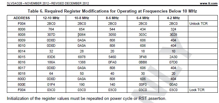
I’m not having much luck communicating and am about 90% sure it has to do with clock rates.  From the datasheet I know the chip takes two clock signals, SCK (SPI input clock), and FCLK (flash clock).  I know the max frequencies are 10 MHz and 12 MHz respectively, and that the flash clock to SPI clock ratio must be 6/5 or higher.  The datasheet also states that “operation below 10 MHz acceptable."


So the questions I have are:

1)      Is the 10 MHz lower operating limit for SCK or for FCLK?

2)      what are the absolute min SPI clock and flash clock frequencies, and what sort of config changes are required?


Thanks,

Ryan

  • Ryan,

    The 10Mhz is relative to FCLK.   Operating below 10Mhz requires config changes.

    SPI clock can be any frequency, as long as it is less than 5/6 of FCLK.

    Here is the section of the draft datasheet that will include the details.  There are several updates underway, and this should be on the web early in Jan.

    ---

    Provisions for Operating With fCLK Frequencies Less than 10 MHz
    The SM28VLT32 uses a state machine and registers to implement the correct algorithms for programing, erasure
    and validation. The register values define counters and loops that determine appropriate setup and hold times,
    maximum attempts, pulse widths, and other critical parameters. The default values of these registers are defined
    for fCLK operation in the 10 MHz to 12 MHz range. Operating below 10 MHhz requires changing key registers to
    properly implement the algorithm. See Table 6 for register settings for specific fCLK ranges. Note, the 10 MHz to
    12 MHz values are provided, but are not required to be written as they are the reset defaults. Additionally, the
    SPI SCLK frequency must be 5/6ths of fCLK or slower for reliable operation.
    The values below represent the address and value that should be written using the 1D command. Note that first
    line is a write to F004. This must be first, as it unlocks the test control register and allows modification of the
    memory mapped registers. Without this write, the contents of the register would not change. It is recommended
    to follow the register writes with a read to verify that change was properly implemented. The last line is a write
    back to the test control register to relock it preventing accidental modification of the registers.

  • Hi Ryan and Wade,

    Thanks Ryan for posting my original question to the forum. And thanks Wade for the quick response.

     I'm still having trouble communicating with the flash, and have been looking through various forum posts with no luck.

    What I am trying to do is communicate with the sample SM28VLT32-HT using a TMS320F28335 (clocked at 90MHz). I should also mention I am using SYS/BIOS, so do not do any PIE initialization.

    In SYS/BIOS there have a function bering called every 5 seconds that is supposed to get the flash status.

    I've scoped all inputs and outputs and everything seems to be being sent to the flash as expected, but I am receiving a zero from the flash when sending a 0x22 (read status register command). SCK is 9.009MHz, FCLK is 11.42MHz. HOLD, WP, and CS are acting as exptected. I can see the data being sent to the flash onto the SI pin, and see a the flash response on SO, but the value is zero when debugging.

    Is there any more detailed information about the commands and responses from the SM28VLT32-HT?

    Here is the relevant code.

    main

    {

    ...

    InitGpio(); // includes setting SPI GPIO, manually controlling SPISTEA on GPIO57

    spi_fifo_init(); //init the SPI FIFO

    spi_init();  // init the SPI registers

    BIOS_start();

    }

    void spi_fifo_init()

    {

    // Initialize SPI FIFO registers

    SpiaRegs.SPIFFTX.all=0xE040;

    SpiaRegs.SPIFFRX.all=0x2041;   

    SpiaRegs.SPIFFCT.all=0x0;

    }

    void spi_init()

    {  

    SpiaRegs.SPICCR.all =0x0007;                 // Reset on, rising edge, 16-bit char bits  <-- changed to 8-bit (was 0x000F  

    SpiaRegs.SPICTL.all =0x0007;                // Enable master mode, normal phase,                                                 // enable talk, and SPI int disabled.  

    SpiaRegs.SPIBRR =0x0004;  

    SpiaRegs.SPICCR.all =0x0087; // was 9F for loopback mode;                // Relinquish SPI from Reset8f  <-- was 8f for 16-bit  

    SpiaRegs.SPIPRI.bit.FREE = 1;                // Set so breakpoints don't disturb xmission

    }

     Every 5 seconds I attempt to read the flash status.

    void getFlashStatus()

     {  

    Uint16 sdata, sdata2;  // send data  

    Uint16 rdata, rdata2, rdata3;  // received data  

    sdata = 0x0022; //read status register  

    sdata2= 0x0000; //dummy data  

     EALLOW;  

    FLASH_SET_WP_HIGH;  

    FLASH_SET_CS_LOW;  

    EDIS;

     rdata2 = SpiaRegs.SPIRXBUF;      //this will Clear the RX interrupt flag  

    SpiaRegs.SPIFFTX.bit.TXFFINTCLR = 1;    //Clear the TX FIFO interrupt  

    SpiaRegs.SPIDAT = sdata << 8; //send the 8 MSB  of the status command

    //while ( SpiaRegs.SPISTS.bit.INT_FLAG != 1) {} //Wait for byte to be shifted out  

    while ( SpiaRegs.SPIFFRX.bit.RXFFINT != 1) {} //Wait for byte to be shifted out  

    rdata = SpiaRegs.SPIRXBUF;  

    SpiaRegs.SPIDAT = sdata2; //send the first dummy byte  

    while ( SpiaRegs.SPIFFRX.bit.RXFFINT != 1) {} //Wait for byte to be shifted out  

    rdata2 = SpiaRegs.SPIRXBUF;  

    SpiaRegs.SPIDAT = sdata2; //send the second dummy byte  

    while ( SpiaRegs.SPIFFRX.bit.RXFFINT != 1) {} //Wait for byte to be shifted out  

    rdata3 = SpiaRegs.SPIRXBUF;

     EALLOW;  

    FLASH_SET_CS_HIGH;  

    FLASH_SET_WP_LOW;  

    EDIS;

    }

    rdata, rdata2, and rdata3 all contain 0.

    Any suggestions?

    Thanks,

    Bruce


  • Bruce, my first thought would be that you are not powering up appropriately.

    Have you verified the VCore and VIO supplies?   Is RST being held low during power up?

    Could you provide scope shots of the power up (VCORE, VIO, RST) , and of the 0x22 transaction for nCS, SCLK, SI, SO.    Assumption is that WP and Hold are logic high at point of communication.

    I am also assuming that FCLK is continuous clock, and not disabled when not talking to device.

    You can post information here, or send directly to my email at w a d e v b (at) t i . com.   (no spaces).
    Regards,

    Wade

  • Hi , 

    This information is very useful. I have got communication to work with FLCK = 12MHz, SCLK = 6MHz but would like to lower the chip clock rate to save power so need to change it to 4 - 2 MHz.

    when it says "Initialization of register values must be repeated on power cycle or RST. Does this mean every time I turn of the Flash or reset it, I need to have the clock set to 12MHz send the above commands before changing the clock back to the lower frequency?

    just to confirm the above command would be sent as follows 1D 00F004 2BC0 , 1D 00 008006 0324 ....... ending in 1D 00F004 03C0. after the last instruction is sent , the clock can then be changed to 4 - 2 MHz ?

    Any help would be much Appreciated,

    Neil 


  • Neil, I should be able to help answer your questions.

    First off, reducing the clock frequency will not significantly decrease current consumption.  Much of the current draw is related to sense amps in the banks of the array.  This is a static consumption.

    However, if you wish to reduce the frequency of communication, you do not need to set to 12Mhz to send the configuration.  You must set the configuration before using the device for any operation.  So, you can communicate and set appropriate registers with lower frequency clock (must meet fclk/spi clk requirement) before reading/writing/erasing the array.

    Finally, to save the most power, you can implement power saving features within the device.   These are discussed in the application note in the product folder:

    http://www.ti.com/litv/pdf/slva550

    Regards,

    Wade

  • Hi Wade, 

    Thank you for your help. just confirm when you say "You must set the configuration before using the device for any operation". Does this mean that the chip I'm currently working with where Ive been writing/reading and erasing segments at 12Mhz Fclk can now not be re-configured for 2 - 4 MHz ? or did you mean after the chip power up sequence  it must be configured before using it for any operation.

    Regards,

    Neil


  • Neil, the latter. The device will function at lower frequencies after configuration change.

    Operation at lower frequencies without the configuration change can damage the device due to potential over erase and/or over programming.

    The configuration essentially sets the internal FLASH access timings to be correct for the frequencies in the table.

    Regards,

    Wade

  • Hello

    I modified my circuit board below:

    1)      Elevated the Vcore to 1.9V

    2)      The oscillator to supply the clock signal for the FLCK is replaced with a new one which the frequency is 11.0592MHZ .

    3)      Soldered a pull-down resistor (5.1k) for the RTS pin and inserted a switch between the RST and MCU I/O in order to guarantee that the RST is low during power up.

    Note: after the flash power up, turn on the switch, the MCU can control the RST.


    The MCU to communicate with the sample flash(rev2.0) is microchip’s PIC18F46K22, the MCU system clock is 32mhz and the SPI clock is 8MHZ.

    Q1:

    I can correctly read and write internal timing registers. But I always get the 0x0000 when I read the status register with the command 0x22.

    Here are the code to initialize the SPI and read status register:

    void Init_SPI1(void)

    {

        PMD1bits.MSSP1MD = 0;   //Eanble SPI1 module

        SSP1CON1bits.SSPEN = 0;

        SSP1STAT = 0x00;          //SKE = 0

           SSP1CON1 = 0x30;         //SPI master mode, clock = Fosc/4, idle clock is high

        SSP1CON3 = 0x00;

           PIR1bits.SSP1IF = 0;              //Clean SPI interrupt flag

           IPR1bits.SSP1IP = 0;              //Clean SPI interrupt priority

           PIE1bits.SSP1IE = 0;              //Disable SPI interrupt

    }


    unsigned short Read_StatusRegister(void)

    {

           unsigned char ucTempData;

           unsigned char usStatusWord = 0;

           WP_FLASH = 1;       //WP goes high

           CS_FLASH = 0; //CS goes low

           ucTempChar = SSP1BUF;              //Clean BF

           SSP1BUF = 0x22;      //Transmit command

           while(SSP1STATbits.BF == 0);      //Waiting for if transmit does not end

           ucTempData = SSP1BUF;       //Clean BF

           SSP1BUF = DUMMY_DATA;      //Transmit recieve clocks: dummy byte

           while(SSP1STATbits.BF == 0);      //Waiting for if transmit does not end

           ucTempData = SSP1BUF;       //Read data and clean BF

           usStatusWord |= ( ( ((unsigned short)ucTempData) <<8 ) & 0xFF00 );


           SSP1BUF = DUMMY_DATA;      //Transmit recieve clocks

           while(SSP1STATbits.BF == 0);      //Waiting for if transmit does not end

           ucTempData = SSP1BUF;       //Read data and clean BF

           usStatusWord |= ( ((unsigned short)ucTempData) & 0x00FF );


           CS_FLASH = 1; //CS goes high

           WP_FLASH = 0;       //WP goes low

           return( usStatusWord );

    }


    Q2:

    I do not understand the validate segment command (0x1A), could you explain it?


  • Kejun,

    Several comments.

    First off.  Silicon Rev 2.0 has a power supply issue, and is really not the best to use for development.  Especially since Rev 2.1 was just released.

    In order to use 2.0 for checkout only, the Vcore needs to be elevated to 2.8v.   This will drastically reduce the devices life, and it should not be used at temperature.

    When you are at 1.9v for Vcore, the status register should still function and should report back revision ID of 1000.   All other bits will be 0, as the flash array is not enabled (due to the Vcore not being elevated).

    I cannot comment on your code for the PIC controller.    It may be beneficial to probe the CS, SPI clock and data lines to see if proper commands are being sent.

    If you post scope plots, I can take a look and comment.

    The Validate segment command is only necessary if only erasing single segments in a bank.  The banks are organized with segment pairs.  Segments 0-7, 1-6, 2-5,  and 3-4 are matched pairs.   If one segment is erased, but not the other, then the other should be validated to help maintain the matching characteristics.

    If the array is always bulk erased, then this command is not necessary.

    Regards,

    Wade

  • Hi Wade

    I appreciate you for your response, I still have some questions and I hope you do me an favour.

    1) Do you have some further information about the organization of the SM28VLT-32, for example, how many banks or segments does it include?

    2) According to the datasheet and your reply. When I erase a single segment, I must send both the command “validate segment(0x1A)” and the command “erase segment (0x19)”, if my understanding is correct, which command is sent first? you mentioned the bulk erase, I don't find this command, is this command erase a bank or erase full chip?

    3) One quick status register and one status register inside the flash. The status register[7:0] is similar with the quick status register, what suggestions to me when I poll quick status register and when I poll status register?

    4) Can I get two silicon Rev 2.1 samples?

  • Kejun,

    I just discovered that some of these questions were being routed through James Davis.

    Lets address them here instead of multiple paths.   

    1) The SM28VLT32 is comprised of 8 banks with 8 sectors each bank.

    2) There is not a bulk erase, but if you have host erase all segments at the same time, then the validate is not required.   But, if you only erase a single segment, then intend to continue writing to the device, it is necessary to issue the validate command to (at a minimum) the segment that is the erased segments pair. 

    3) I do not understand this question.  Some of your questions may be answered in the application section of the datasheet.

    4) I have let our Marketing team know.  They will have to address this.

    Regards,

    Wade

  • Hi Wade,

    I'm just now getting back into working with the flash and am having some difficulty.

    I don't seem to be able to write to the device or erase the device.

    WS, HOLD, and RST are all high. CS, SCK, FLCLK all look good.

    The results I am seeing are:

    Quick Status   (bin) 00000000 00000000

    Clear Error  

    Quick Status  (bin) 00000000 00000000

    Read Status Reg  (bin) 00000000 00001001

    Write 123 to address 0 (bin) 00000000 00001000

    Quick Status  (bin) 00000000 00000100

    Quick Status  (bin) 00000000 00000100

    Read Status Reg  (bin) 00000100 00001001

    Clear Error  

    Read address 0  (bin) 00000000 00000000, Data=0

    Quick Status  (bin) 00000000 00000000

    Quick Status  (bin) 00000000 00000000

    Read Status Reg  (bin) 00000000 00001001

    Clear Error  

    Write 234 to address 1 (bin) 00000000 00001000

    Quick Status  (bin) 00000000 00000100

    Quick Status  (bin) 00000000 00000100

    Read Status Reg  (bin) 00000100 00001001

    Clear Error  

    Read address 1  (bin) 00000000 00000000, Data=0

    Quick Status  (bin) 00000000 00000000

    Quick Status  (bin) 00000000 00000000

    Read Status Reg  (bin) 00000000 00001001

    Clear Error  

    Your thoughts?

    Thanks

    Bruce


  • Bruce, help me understand your logs.

    You have 2bytes for results of quick status.  This should only be 1 byte.   Is it padded?

    Otherwise, if all else is good, then it looks like the array is all 0's. 

    The erased state should be all 1's   Try erasing and see if you can get all 1's on a read.

    If your data is padded, then the 100 after your write indicates invalid data.  Trying to write a 1 when it is a 0.  this is not possible.

    Regards,

    Wade

  • Hi Wade,

    Yes, the result from the quick status is padded. The 8 LSB is the value. I just copied the bin value from CCS, where it's type is int, thus the 16-bit.

    I am correct in saying that the chip has 8 sectors, each sector has 0x40000 addresses (0x00000 to 0x3FFFF) and that the erase happens for the entire 0x40000 address sector that the 21-bit address belongs too?

    I've tried some erases, I'm not getting 1's on a read after though.

    ErrorCode = Flash_SendFF(); //response is (bin) 00000000

    Flash_ClearError();  

    ErrorCode = Flash_SendFF(); //response is (bin) 00000000

    Flash_ReadStatusRegister(&ErrorCode); //response is (bin) 00000000 00001001

    for (iCnt=0; iCnt<8; iCnt++) {  

    ErrorCode = Flash_EraseSector(iCnt*0x40000); //response is (bin) 00011000  

    ErrorCode = Flash_SendFF(); //response is (bin) 00011000  

    ErrorCode = Flash_SendFF(); //response is (bin) 00011000  

    ErrorCode = Flash_SendFF(); //response is (bin) 00011000 }

    for (iCnt=0; iCnt<8; iCnt++) {  

    ErrorCode = Flash_ValidateSector(iCnt*0x40000); //response is (bin) 00011000

    ErrorCode = Flash_SendFF(); //response is (bin) 00011000  

    ErrorCode = Flash_SendFF(); //response is (bin) 00011000  

    ErrorCode = Flash_SendFF(); //response is (bin) 00011000 }

    ErrorCode = Flash_Read(0, &data); //Errorcode response is (bin) 00000000, data is 0.

    ErrorCode = Flash_SendFF(); //response is (bin) 00011010

    ErrorCode = Flash_SendFF(); //response is (bin) 00011000

    ErrorCode = Flash_SendFF(); //response is (bin) 00011000

    Flash_ReadStatusRegister(&ErrorCode); //response is (bin) 00011000 00001001


     Thanks,

    Bruce


  • Bruce,

    The response 00011000 indicates device busy and erase busy.  You will need to poll until the erase is complete on that sector, then can continue to next sector.  All sectors in a bank should be erased (or validated) at the same time.  There is note in datasheet on this.

    I have a script file with each sector and erase commands.  You can extract the start of all sectors from this.

    Regards,

    Wadehttp://e2e.ti.com/cfs-file.ashx/__key/communityserver-discussions-components-files/30/3386.func1_5F00_erase_5F00_array.seq

    The format of the file is command_address_dummy  

    So it is 19_address_FFFF   You can extract the 3 bytes of address for your erase.

    Regards,

    Wade

  • Thanks for the script Wade. I didn't realize I had to perform that many erase operations to totally erase the flash. It's all working well now.

    Bruce.