This thread has been locked.

If you have a related question, please click the "Ask a related question" button in the top right corner. The newly created question will be automatically linked to this question.

ADS8556 EVM can't obtain BUSY signal

Other Parts Discussed in Thread: ADS8556, TMS320C28346

Hello, everyone.

I meet some problem right now, that is I can´t obtain the BUSY signal from the ADC.

I´m a master student doing my final project right now. I´m using a DSP of TMS320C28346 Experiemnter´s kit to control a AC/DC power rectifier. Since there is no ADC integrated on 28346 control card, we purchased your ADC of  ADS8556 EVM. I´ve programmed the external interruption through  one GPIO pin of the DSP( this pin later will be connected with the BUSY signal from the ADC),and this external interruption interrupts the CPU precisely.

Now the problem focused on the ADC EVM. I wanna use it in hardware and parallel controlled mode. So that @210kHz, I wanna measure the input voltage of my power rectifier and send the digital 16-bit data all together to the DSP through GPIOs.

Now my testing condition is :

--Analog input channel  A0 A1 B0 B1 C0 C1 all connected with the analog ground pins next to them.(just to make things simple)

--A start of conversion PWM signal @ 210KHz is generated from DSP to the ADC to trigger the data conversion.

My  configuration is as below:

--For power supply of the  ADC board,

I connect +12V to J3.1, -12V  to J3.2, +5V to J3.3,  and J3.6 connects with the common ground for both +-12V and +5V .

As for the digital supply part, I supply J3.9 with +3.3V and J3.5 with the groud of +3.3V, of course the ground of the former analog part is isolated with the ground of 3.3V part. And also the jumper JP4 is placed to the right, connecting with the 3.3V pin.  Rest of the pins in J3 are left unconnected.

For the supply part, I´ve checked all the test points, they are; TP1: -12V, TP2: +12V, TP14: AGND 0V, TP3: +5V, TP8: nothing(because by JP4, .3.3V is connected as BVDD), TP16: +3.3V . Also the diodes D1 & D2 are on perfectly.  So I believe the supply part shouldn´t cause any problem.

--For the SW1 part, I did as default in this EVM user´s guide, all the switches turned to the right except for the last one(REFen) to the left.

Of course, JP12 is well placed because I  wanna use the internal reference and also I can measure at the TP10 2.5V and TP11 0V perfectly.

--For the other jumpers,

JP1,2,6,7,5,8 are all connected with its Pin2 and Pin3,.Even though in the user´s manual it´s said by default should be Pin1 and Pin2. I´ve ried both ways, none of them worked.

JP10 and 11 are also well placed and I can measure +12V and -12V separately on them.

For JP3, only the first row J1.7 is placed so that  /CS signal is connected with J1.7  (tied together with J1.9) in serial control ports. Also I wired J1.9 and J1.10 so that /CS is kept ZERO forever. The rest  Y1 Y2 and Y3 are unplaced. 

For JP9 I place three jumpers between HOLD A/B/C and DC_TOUT individually. And also I connect the start of conversion signal from DSP to this DC_TOUT  in Parallel control ports. Of course I can measure exactly the same start of conversion pulse on HOLD A/B/C since they are tied together.

--For the Parallel Control Ports,

I make DC_A0 and DC_A1 floated HIGH, DC_A2 connected with the digital ground beside it. Thus for the A B C inputs in the U3(multiplexer), I have a HIGH HIGH LOW logic. Plus, for DC_A3, I supply a constant HIGH from one of the DSP GPIO pin, so that G1 in the multiplexer is measured HIGH. For DC_CNTL( connecting with /G2A in multiplexer), I didn´t do anything, and it´s measured LOW. Besides, /G2B is originally LOW. Above all, according to the truth table of the multiplexer, I should have the output Y7 pin HIGH, which gives the /STBY signal to the ADC chip.  And I measured Y7 pin from multiplexer, it is HIGH. That means at least I didn´t make the ADC into shut-down mode :P

For the DC_AWE pin, I didn´t do anything either because I don´t want to write at all. 

For the DC_ARE# pin, it´s connected with a GPIO pin on DSP so that once the falling edge of the BUSY signal occurs, the DSP jumps into this external interruption and inside the interruption enables  this DC_ARE#( /RD in ADC chip )LOW  while acquiring conversion data DB[0:15] to a set of 16 GPIO input ports, and toggles HIGH after data acquisition.

In the very end, I measure the DC_INTa(connected with BUSY from ADC chip) and there is nothing but always 0. 

Since there is no BUSY pulse from ADC, right now I didn´t connect the DC_INTa with the assigned external interruption GPIO port. Because I think there is no way that DSP would jump into the external interruption with a constant ZERO BUSY signal...

That is pretty much what I´ve done up to now.

Please help me figure out if there is anything wrong with my story or can you please tell me how can I obtain the BUSY signal of the ADC, at least by a simple test to verify that my ADC EVM is not dead.

Thank you so much and looking forward to your reply.

Sisi

  • Hi Sisi,

    Welcome to our e2e community!  By the verbal description above, it sounds like you have everything connected properly.  How do you have the TMS320C28346 controller ground tied back into the ADS8556 EVM?  Also, there is a RESET input on J1.1 - have you tried pulsing that input high and then returning it to low?

  • Hello Tom!

    Good to hear from you!

    First, of course I have tied the GND of my DSP board together with the digital ground of the ADC board with a wire.

    As to the second point of your suggestions, I can't agree more!!! I tried this just before I saw your respond :P

    Cause I also noticed the J1.1 RESET pin which resets the internal control register as default and I tried to use a logic HIGH to touch the RESET pin for a moment and then release. Surprisingly, the BUSY signal shows up!!!

    But the problem is that every time after I power on the ADC, there is no BUSY signal existing until I touch that pin. 

    Is it normal? 

    Huge thanks for your help!

    Sisi

  • Hi Sisi,

    Great news!  The ADS8556 has an internal power on reset cell (POR) that is normally activated when you apply power to the device.  I've seen a few occasions when the POR does not completely 'reset' and the part appears to be stuck (i.e. no BUSY).  So far, I've not determined the exact sequence to get into this state, but toggling the RESET pin does revive the part.

  • Hi Tom, it's me again. 

    Thank you for your advice before, and we've made the ADC work properly  and it's able to measure perfect sinusoidal voltage as we want.

    Here comes the problem, as I mentioned before, we are sending the data acquired by ADC into DSP and then the DSP calculates the duty cycle for the switches. Next, the switches control a three phase PWM rectifier switching at 210KHz. Before, I was connecting a short piece of wire on the pin J1.1(RESET pin). When we are testing the prototype of the rectifier, in the beginning we are putting small amount of power at the three phase input, and everything is working fine. Later once we increased the input voltage as well as the input power, the ADC stopped working and there was no busy signal at all, Thus, I had to toggle the other end of the wire with an on board 3.3V(Logic HIGH) pin and then release it. 

    However, this was not a good way to operate, because we suspected that the piece of wire with floating end was acting like an antenna and it absorbed so much noise from our power stage.

    In comparison, we get rid of the wire connecting with that reset pin. Only when ADC runs out of operation, I connect the wire and toggle RESET pin. This is time it's better  , we can increase the power more than before. But still, before we can reach the nominal operating input power, the ADC died.

    We really don't know how we can take some measures to protect than RESET pin from switching  noises and also make it revive as soon as the ADC died.

    Plus, we are sure that the analog input voltage we are measuring does not go beyond the range of ADC.

    Do you have any suggestions? Thank you so much!!!!

    Sisi

  • Hi Sisi,

    If you can send along the Gerber files of your board, we'll take a look at the layout for you.

  • Hi Tom, 

    Sorry we can not offer your our gerber files. but I can describe more or less our layout with a draw later.

    Right now, our problem is still with the ADC. Our rectifier can only work well at very low power(around 10W, while the nominal power is 2kW). Once we tried to increase the power, there seems to be some kind of noise entering into the ADC and lead the ADC into reset mode(i.e. receiving  an external start of conversion signal from DSP, there is no BUSY signal, nor conversed data out of the ADC). We found our ADC so sensitive, even a switch on and off of a power supply nearby( of course not supplying for itself), it will get into a reset mode. Thus we have to toggle the J1.1 RESET pin to revive it every time it happens.

    One thing we found curious is about the digital supply for ADC. Right now we can only supply the J3.9 pin (BVDD) with +2.5V or +2.6V regulated DC voltage, but refer to the ADS8556EVM user´s guide, this pin should be supplied with a +3.3V. The thing is,  when we only try to increase this BVDD supply starting from +2.5V, ADC is dead at around +2.9 volts. This means we can never reach +3.3V. Note that there is an alternative to supply BVDD with +5V on pin J3.10 (of course jumper JP4 in its corresponding position), we also tried this condition. It can not work with +5V supply for digital part., either.

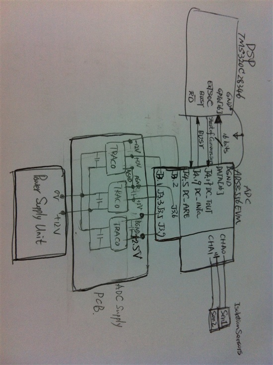
    For the power supply of the ADC, we are using three isolated TRACO converters with capacitors at the input and output of TRACO, to supply isolated +-12V, +5V and +2.5V. 

    The system schematic is drawn as below, 

    Please help us find out where the problem might exist.

    Huge thanks!

    Sisi

  • Hi Sisi,

    This really sounds like a grounding issue.  The BGND and AGND of your supplies need to be at the same potential as the GND of the DSP board and the ground of your analog inputs.