This thread has been locked.

If you have a related question, please click the "Ask a related question" button in the top right corner. The newly created question will be automatically linked to this question.

ADS8344 first conversion

Other Parts Discussed in Thread: ADS8344, TMS320F28335

Hi,

I'm using an ADS8344 in external clock mode, no power-down between conversions.

It seems the very first control bits after power-up of the device are not followed by a correct conversion output.

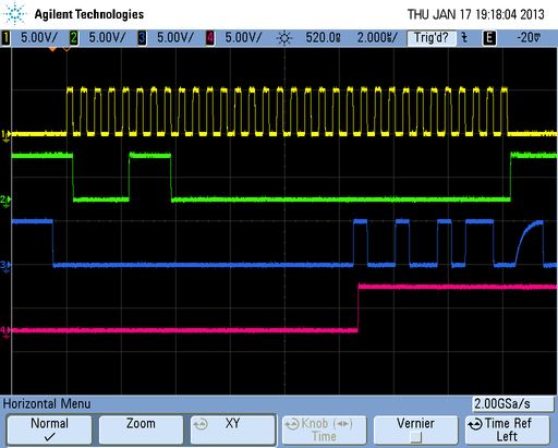
On the image above DOUT is the red channel at the bottom, DIN the blue one, DCLK the green one and the yellow trace is CS.

As we can see, DOUT output some bits even when receiving the first control sequence (channel 0) on DIN, then it seems there is only zeroes as the conversion result. The next control bits (channel 1) are followed by the correct conversion value on DOUT. All next channels are correctly converted.

Is it due to a clock mode change because the ADS8344 was in internal clock mode at power-up? The datasheet doesn't seem to mention which mode is selected by default at power-up.

Thanks in advance for any comment.

Regards,

Eric.

  • Hi Eric,

    According to the datasheet:
    1) the clock mode must be set explicitly after power is first applied to the device
    2) the desired clock mode is effective in the conversion cycle that follows the "extra" cycle needed for 1)

    It sounds as though your external clock mode setting is taking effect after the first conversion cycle. However, the clock mode during the first cycle is unknown. What is the state of the BUSY signal during the first conversion cycle? From figure 6, if the internal conversion clock is being used then BUSY should be high during this period. Could you please also send me your schematic and the conditions you applied on your analog inputs and power supply to produce the plot? I will try to replicate your observations in our lab.

    Thank you.

    Best Regards,
    Harsha Munikoti

  • HI Harsha,

    Thanks for your answer. I needed some time to make new plots with known analog inputs and to be sure it was the very first acquisition. But it seems I didn't read carefully enough the datasheet about - clock mode - then power-down mode - programming through the PD bits on page 13.

    The following plots illustrate that we make 8 acquisitions in single mode from channel 0 to 7, wich implies to send on DIN adresses 0, 4, 1, 5, 2, 6, 3, and 7.

    CS is plugged on external trig of the scope. Scope channel 1 is DCLK, ch2 is DIN, ch3 is DOUT, ch4 is BUSY.

    The first plot is the first acquisition, the next one the second acquisition.

    The two analog inputs present the same voltage measured with a multimeter on the pins 1 and 2 of the ADS8344 = 2.88V.

    (analog inputs pin 3 to 8 : 2.88V 1.91V 2.23V 3.32V 2.55V 2.15V)

    The second acquisition seems correct as I read 0x9247 for the sample : 0x9247 / FFFF x 5 volts = 2.86V. The first acquisition is obviously much smaller and BUSY doesn't beahve as in external mode.

    The following plot is the entire set of 8 acquisitions :

    Here is the schematics  I put it as "Insert file" I hope it is readible. :

    I think you pointed out the problem we encountered in your first answer, but if you have any new comments I would really appreciate them. If you try to reproduce the behaviour in your lab, I'd be happy to answer your next questions if any.

    I believe there is no way to impose an external clock mode from power-up, and so we need to add one first "dummy" acquisition, do you agree with this? The DSP we use is a TMS320F28335 which interfaces the ADC through a MCBSP function.

    Thanks a lot for your rapid and usefull answer.

    Best regards,

    Eric.

  • Hi Eric,

    Thank you for the detailed information.

    The state of BUSY during the first conversion cycle indicates that the ADC is not converting, and as a result the data output is not a valid conversion result. The reason is that the conversion clock for the ADC (internal or external) is not enabled after power-up. Only after the first conversion cycle, the desired clock mode is selected and enabled.

    As you have pointed out, the data output produced during the first "dummy" conversion cycle should be ignored.

    Please let me know if I can be of any further assistance. Thank you.

    Best Regards,
    Harsha