This thread has been locked.

If you have a related question, please click the "Ask a related question" button in the top right corner. The newly created question will be automatically linked to this question.

DAC8811 EVM noise issue

Other Parts Discussed in Thread: THS4031, OPA277, DAC8811, THS4032

Hi,

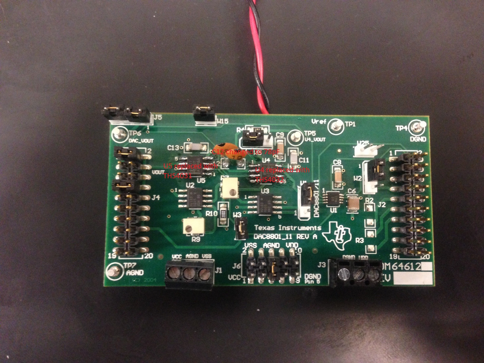
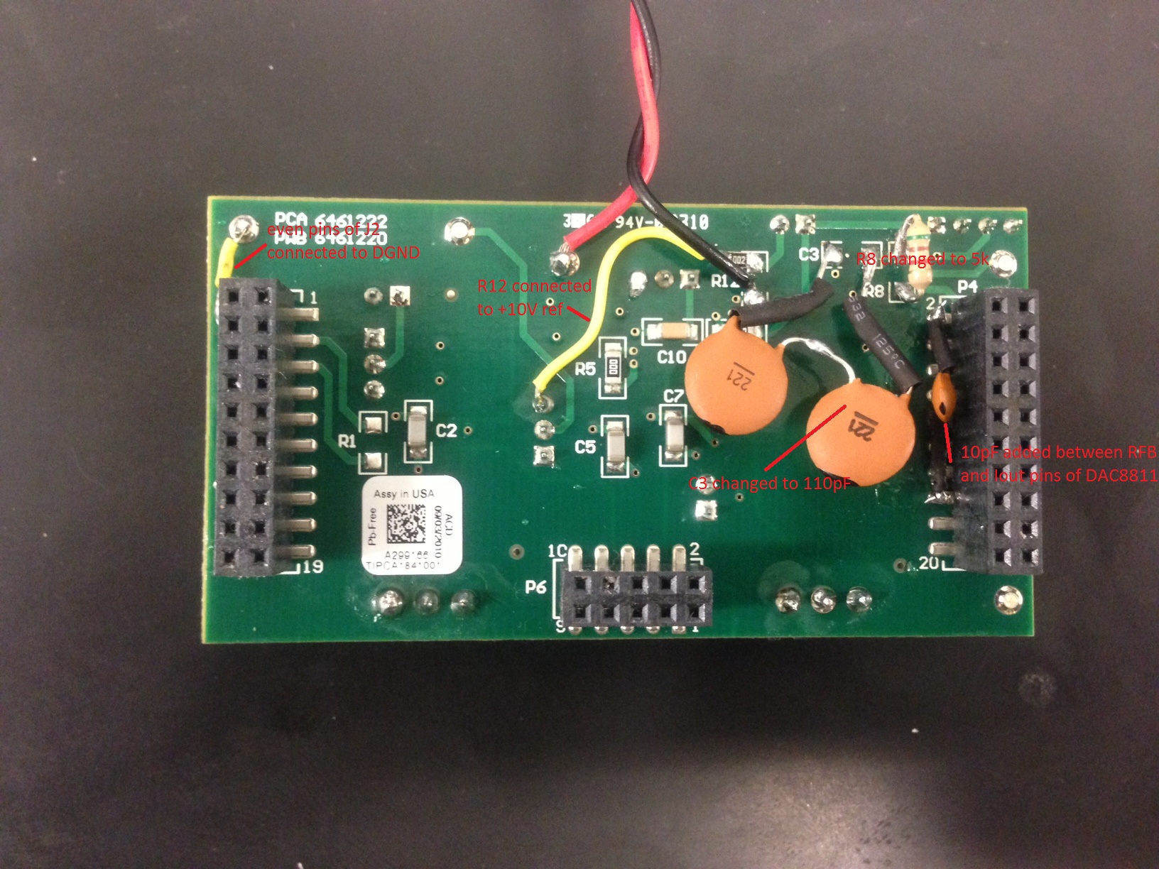
        I'm using the DAC8811 EVM, a 16-bit serial input multiplying digital-to-analog converter, in my system for +/-10 V analog output. A DE2-115 (Cyclone IV) FPGA board from altera is used to interface with this EVM and generate CS, SCLK and SDI signals according to the timing diagram of DAC8811. To achieve +/-10V bipolar output, the configuration of this EVM is changed to Fig. 22 in the datasheet of DAC8811 with +10V ref voltage. Also, the original OP on the EVM board (OPA277) is changed to THS4031 for faster slew rate.

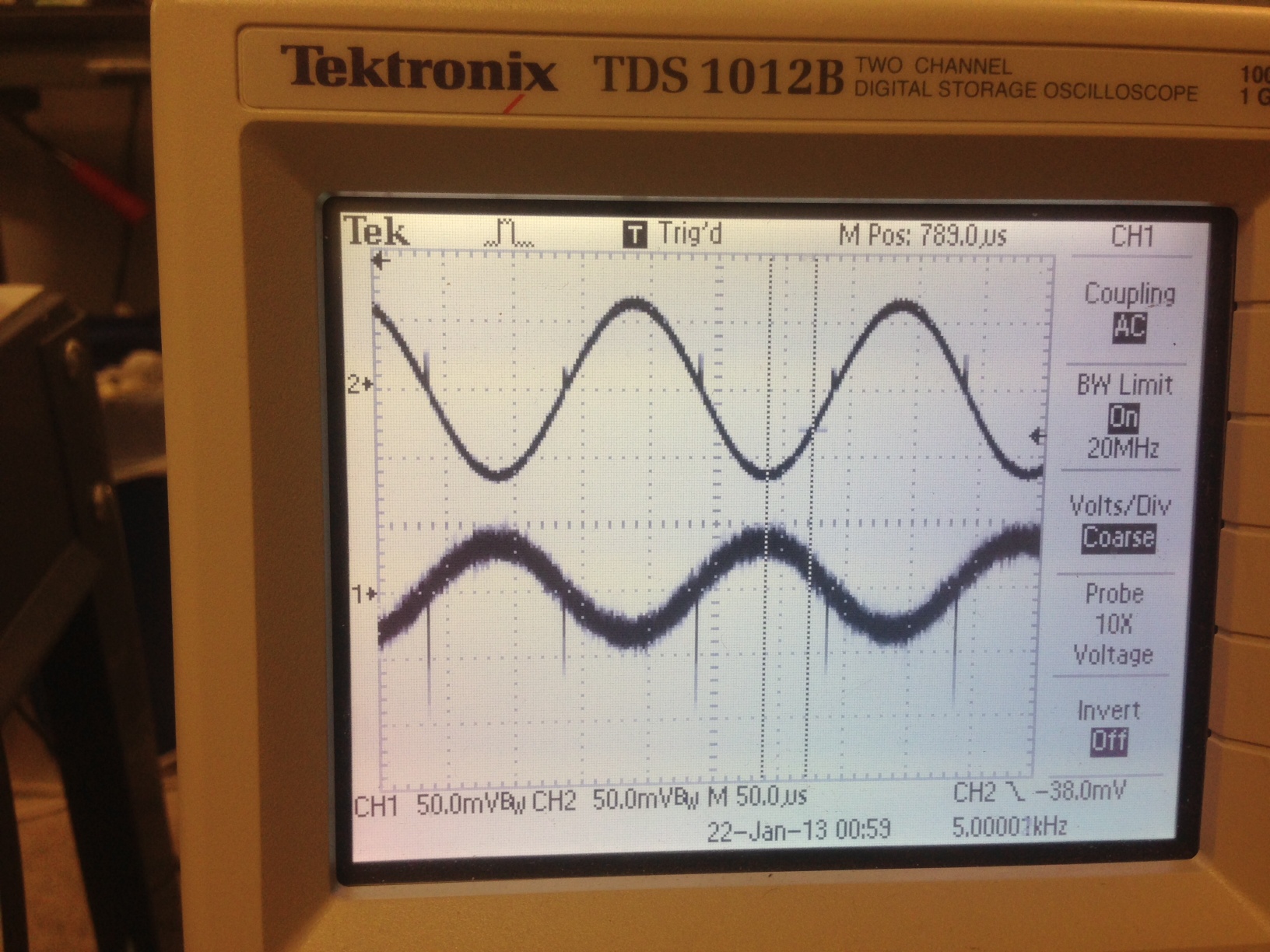
        The analog output from this EVM now is pretty noisy and has sharp glitches at zero-crossing point, as can be seen in the attached picture (noisier wave is the output of U5 and the cleaner wave is output of U4A with low-pass-filtered output). Please suggest how I can suppress the noise in the output and eliminate the zero-crossing glitch.

        I'm applying the following power supplies to the EVM:

        VCC: +12V; VSS: -12V; VDD:+5V (VDD is from the FPGA board)

Regards,

Zhen Liu


  • Zhen,

    I'm working on getting my hands on an EVM to replicate your setup. Did you cut a trace to create a summing configuration at U4A? Also, looking at your scope shots the voltage divisions look to be 50.0mV but you said you're creating a +/-10V signal. What's going on there?

  • ...also did you change out both U5 and U4A with THS4031s?

  • Hi Kevin,

    I cut the trace from R12 to ground and connected the +10V ref on board to R12. My objective is to provide a +/-10V swing range. But for this test, I just generated sinusoidal wave with about 150mv peak-to-peak value to show the noise and spike.

    All the modifications I made on the EVM are as follows:

    1. Change U5 to THS4031 and U4 to THS4032 for faster slew rate, although I indeed notice these two ops have relatively large input offset voltage.

    2. Add 10pF capacitor between RFB and Iout pins of DAC8811 to improve stability

    3. Change R8 from 2k to 5k for summation and change C3 from 470pF to 110pF so that the LPF bandwidth be 289.5kHz

    4. Connect R12 to +10V ref

    5. Change C12 to 78pF so that the LPF bandwidth in the U4A feedback network is 204kHz

    6. Connect all the even pins of J2 to digital ground.

    The attached pictures show the top and bottom of modified EVM, from which the jumper settings could also be seen:

    Really appreciate your help. Thanks.

    Regards,

    Zhen Liu

  • Pictures with bigger notation for your reference. Thanks.

    Zhen Liu

  • Zhen,

    I replicated this real quick today, I didn't modify any of the capacitor values but changed the series resistor to the output buffer and created the summing structure off of the reference. I do see a pretty noisy signal out of the transimpedance amplifier that does show quite dominant zero-crossing glitches but with the capacitor values on the board by default I do not see these glitches on the output. Why did you move the cutoff for you filters so far out? It looks like you're creating a signal ~10kHz.

  • Hi Kevin,

    The signal I showed in the test was 5kHz, but the frequency range I hope to generate using this DAC falls between 1kHz and 50kHz. Therefore I changed the capacitor values. With the default capacitors, the LPF bandwidth in the output buffer is just 16kHz, too low for my application.

    Do you have any idea why the signal out of the transimpedance amplifier is so noisy and has the zero-crossing glitch? I feel the analog signal might be contaminated by the digital noise since I observed SCLK frequency component in the analog output. Also, in your replication, did you change the ops to THS4031 or just use the original ones? 

    Thanks.

    Zhen Liu

  • Zhen,

    I changed the amplifiers to THS4031/2s. I didn't spend much time looking at the noise characteristics of the original amplifiers, and I regret that.

    Some of the noise we see from the transimpedance amplifier could be due to the offset voltage being higher on the THS devices as you mentioned earlier. This creates a sort of modulation effect on the output of the system that results in degraded linearity which could manifest itself as noise. Generally speaking our precision data converters are targeted for DC applications. Noise sources in transimpedance amps is extremely tricky. I'm far from a transimpedance amplifier expert but Bob Pease wrote a pretty good short article about transimpedance amplifiers and points to resistor matching, the feedback resistor, source capacitance, bandwidth considerations, gain, voltage and current noise of the amplifier, input capacitance of the amplifier, and gain-bandwidth product as dynamic contributors to this equation. With the DAC being in there we're going to see dynamic resistor matching and source capacitance that's just going to exacerbate things.

    What you mentioned about the SPI CLK feeding through is a possibility as well, digital feedthrough can be observed in a number of DAC architectures.

    There are techniques as well that you can look at to removing the glitch entirely. I've seen track and hold circuits and sample and hold circuits implemented to smooth out glitch energy, but I don't have anything handy and written up for you to read already. I'll think on this for a bit and try to come up with something simple to try...on the whole though I think there may be better solutions out there to generate cleaner AC signals.