This thread has been locked.

If you have a related question, please click the "Ask a related question" button in the top right corner. The newly created question will be automatically linked to this question.

Some trouble about IDACs

Other Parts Discussed in Thread: ADS1147

Hi all,

First, I'm very sorry for my English.

And the second,

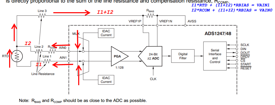
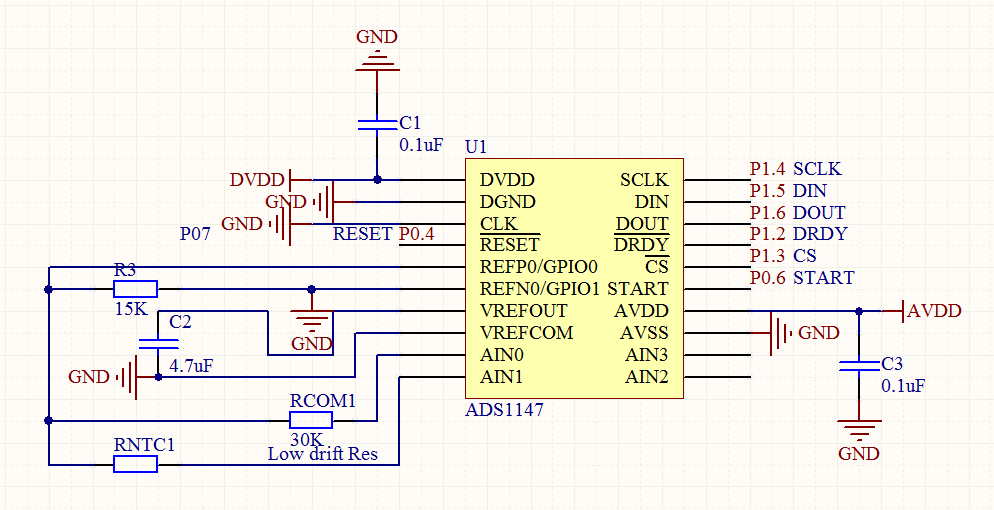
In the accordance with the Three-Wire RTD Application with Hardware Compensation of SBAA180 of ADS1147(see below), the red line was marked is the direction of current, and use the RBIAS to produce external reference voltage.

My setting as follow:

The NTC range is 3.75KΩ to 52.3K

RCOM:     30K

RBIAS:     15K         because I want to use external reference voltage of 1.5V

AVDD:        3V

AVSS:                   0V

PGA:           1

IDAC(AIN0,AIN1):              50μA

Data rate:                   5sps


The problem is: when the resistance value of NTC less than 30K,the external reference voltage is kept at about 1.5V, this is acceptable.But when the NTC value greater than 30K.the reference had droped severely,such as 1.2V, 1.07V and so on.Can you tell me something wrong about my schematic,setting and why the IDAC can fall.

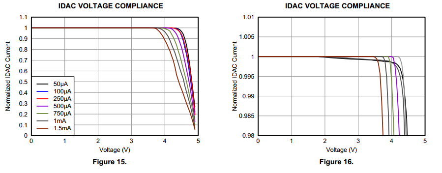
By the way,can you explain Figure 15 and 16 for me? The voltage means what? AVDD or others?

Best regards,

Penn

  • Hi Penn,

    Welcome to the forum!  The graphs you refer to are showing that relative to the supply voltage (which in this case is 5V) your output current from the IDACs becomes restricted when the voltage produced from the resistance/IDAC combination starts to approach the supply voltage.  From the datasheet electrical characteristics table, the typical compliance voltage reduction from the supply is 0.7V.  This means that the maximum voltage drop from any currently source output to AVSS for a 3V analog supply is 2.3V.  If the reference resistor has a 1.5V drop, this means you can only have 0.8V drop across the RComp or thermistor resistance value.  50uA through 30k ohms is 1.5V, plus 1.5V reference voltage is 3V.  This is out of compliance and it will not be possible to sustain (or start) a constant current.

    Generally it is a good idea to maintain some margin, so you might want to redesign your project to either increase the AVDD voltage, lower the reference voltage, or both.  It is better to design the system so that the maximum voltage drop is AVDD-1, so if you maintain 3.0V for AVDD, the maximum voltage drop should only be 2.0V from the IDAC source to ground.  The minimum reference voltage is 0.5V, so if you reduce the reference bias resistor to 5K, and leaving RComp at 30k, the total voltage drop will be 2V from AIN0.  AIN1 will vary, and you will be ok up to 30k, but you will be marginal above (larger than) 30k.  At 36k you will be out of compliance for sure.  In this case using a higher voltage for AVDD would be a better choice.

    Best regards,

    Bob B

  • Thank you so much for help,However the compliance voltage is a new concept of hard to understand for me.Could you give me some common interpretations about it?

    I really appreciate it.

    Regards,

    Penn

  • Hi Penn,

    Basically the current source requires a voltage to operate and for the circuit to maintain a constant current the resultant voltage can not go beyond a particular voltage drop.  For example, if I have 1mA of current and connect it to a 10k ohm resistor I would get a voltage drop across the resistor of 10V.  You can't get extra voltage when the supply is 5V, so the current source is only able to supply up to the compliance voltage for the specified current range and applied AVDD.

    Best regards,

    Bob B

  • Hi,

    I found that I had a really ridiculous question about the compliance voltage.

    Thanks a lot and best wishes for you.

  • Hi Bob,

    I have another qusetion about the IDACs that we discussed again.

    Though I know that "the current source requires a voltage to operate and for the circuit to maintain a constant current the resultant voltage can not go beyond a particular voltage drop" ,however,if I make some setting as follow:

    AVDD     3V

    AVSS      0v

    IDAC     50uA

    RBIAS   5K     external reference voltage 0.5V

    RCOM  30K  VAIN0 = 2.0V  (Less than 2.3V)

    And when I increase the RTD value from 5K to 50K,although it is illegal. I want to know whether only the current of AIN1 will decline?Or the current of both IDACs always the same?

    Meanwhile,could you tell why 1147 have 3 Single-Ended Inputs?which three input? How do I configure to single-ended input?

    I'm very sorry such a basic question to you.

    Regards,

    Penn

  • Penn,

    The current sources are independent of each other, but if you run one out of compliance, I'm not sure how the device responds overall.

    As far as the single ended inputs, the measurement is always a differential measurement of one input relative to another.  You can make any combination you want, but one of them will have to be assigned to AIN-, while the other three can be assigned to AIN+.  One thing to keep in mind is the common mode input range of the device.  If you want a single ended measurement referred to ground, then you will need to operate the device with bipolar (+/-) supplies.  This is because the input has a buffered PGA stage that will not allow measurements close to the supply rails.

    Best regards,

    Bob B