This thread has been locked.

If you have a related question, please click the "Ask a related question" button in the top right corner. The newly created question will be automatically linked to this question.

is my circuit of ADS1291 right?

Other Parts Discussed in Thread: ADS1291, MSP430F5522, MSP430F5529

hello everyone. I have a problem about ADS1291. Here is my circuit plot


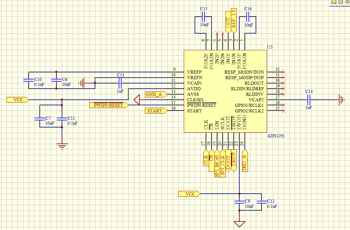
I use the Single-end Input. The input of IN1P is the ouput of an instrument amplifer and the common voltage is 1.5V

and i use the same VCC which is 3V for AVDD and DVDD.

and the same GND for AVSS and DGND.

and i connect the rest pins to a msp430F5522.

But somehow i can't read the correct output .

 i already check the analog amplifer is fine so the input of INIP is fine.

so i am not sure is there something wrong with my ADS1291 circuit or my MSP430 Firmware.

anyone please help me check out my ADS1291 Circuit?

thanks a lot   

  • are you using this chip for ECG application? why you need an amplifier? first you can configure ADS1291 in test mode, and check if you can get 1Hz from your host.

    second you can use scope check PGA1p or PGA1n, see if there are any signal you expect.

    the most important is to setup the registers correct.  what are values of your registers?

    David Sun

  • HI . David.

    i am using this chip for EEG application. That's why i need an amplifier before the ADS1291.

    I don't know what's PGA1P and PGA1N for?

    And i already test this circuit in bread board with Msp430 development Board, and it can work.

    but after the PCB LAYOUT is finished. I test  my PCB (instrument amp and ADS1291)  with MSP430F5522 on another PCB  ,something goes wrong.  I using the external CLK 2.048MHZ for ADS1291 ,and 4MHZ or 4.096MHZ for SPI CLK (i am not sure).  I found that i can't setup the right register .

    Here is my Code and my result about write and read ADS1291 registers.

    #include <msp430f5529.h>
    #include <math.h>

    #define   START            0x80         // P2.7
    #define   PWDN             0xFE         // P2.0

    #define   CS_0             0xEF         // P4.4
    #define   DRDY             0x02         // P2.1


    char RES[24];                               //儲存ADS1291暫存器的值
    char i;

    /*
    disable CS, 開啟SPI介面 3-pin, 8-bit SPI master, MSB  . SCLK=SMCLK/2
    */
    void configure_spi(void)    
    {
      P2DIR |= 0XC1;                            // P2.0, 6, 7 for PWDN, RESET_BT, START
      P4DIR |= 0X1F;                            //
                                                //
      P3SEL |= BIT0 + BIT1 + BIT2;              // P3.0, 1, 2 SPI option select

      P4OUT |= ~CS_0 ;                          // Disable CS    

      UCB0CTL1 |= UCSWRST;                      // **Put state machine in reset**
      UCB0CTL0 |= UCMST+UCSYNC+UCMSB;           // 3-pin, 8-bit SPI master, MSB
      UCB0CTL1 |= UCSSEL_2;                     // SMCLK
      UCB0BR0 = 0x02;                           // /2   8.192/2 =4.096 等於 4.096 = 2*2.048
      UCB0BR1 = 0x00;                           //
      UCB0CTL1 &= ~UCSWRST;                     // **Initialize USCI state machine*

    }


    void main(void)                       

    {

    WDTCTL = WDTPW + WDTHOLD;                 // Stop WDT


      P5SEL |= BIT2+BIT3;                       // Port select XT2

      UCSCTL6 &= ~XT2OFF;                       // Enable XT2
      UCSCTL3 |= SELREF_2;                      // FLLref = REFO
                                                // Since LFXT1 is not used,
                                                // sourcing FLL with LFXT1 can cause
                                                // XT1OFFG flag to set
      UCSCTL4 |= SELA_2;                        // ACLK=REFO,SMCLK=DCO,MCLK=DCO

      // Loop until XT1,XT2 & DCO stabilizes - in this case loop until XT2 settles
      do
      {
        UCSCTL7 &= ~(XT2OFFG + XT1LFOFFG + DCOFFG);
                                                // Clear XT2,XT1,DCO fault flags
        SFRIFG1 &= ~OFIFG;                      // Clear fault flags
      }while (SFRIFG1&OFIFG);                   // Test oscillator fault flag

      UCSCTL6 &= ~XT2DRIVE0;                    // Decrease XT2 Drive according to
                                                // expected frequency
      UCSCTL4 |= SELS_5 + SELM_5;               // SMCLK=MCLK=XT2


      configure_spi();                                                              

      P2OUT &= PWDN;                          //p2.0=0(Low)
      P2OUT &= ~START;                        //p2.7=0(Low) START=0
      P2OUT |= ~PWDN;                         //p2.0=1(High)

      P4OUT &= CS_0;                        // CS=0 CS Enable
     
      while (!(UCB0IFG&UCTXIFG));            // SDATAC
      UCB0TXBUF = 0x11;
        
      while (!(UCB0IFG&UCTXIFG));             //從01h開始寫
      UCB0TXBUF = 0x41;
     
      while (!(UCB0IFG&UCTXIFG));             //寫3個暫存器
      UCB0TXBUF = 0x02;
     
      while (!(UCB0IFG&UCTXIFG));       // WREG CONFIG1 0x03   00000011  continuous mode, Data rate = 1KSPS
      UCB0TXBUF = 0x03;
     
      while (!(UCB0IFG&UCTXIFG));             // WREG CONFIG2 0xA0   10100000  internal reference 2.4 V
      UCB0TXBUF = 0xA0;
     
      while (!(UCB0IFG&UCTXIFG));             // WREG Lead-Off Control Register 0x10   00010000
      UCB0TXBUF = 0x10;
     
      while (!(UCB0IFG&UCTXIFG));            //從04h開始寫
      UCB0TXBUF = 0x44;
     
      while (!(UCB0IFG&UCTXIFG));            //寫兩個暫存器
      UCB0TXBUF = 0x01;
       
      while (!(UCB0IFG&UCTXIFG));             // WREG CH1     0x10   00010000    
      UCB0TXBUF = 0x10;

      while (!(UCB0IFG&UCTXIFG));             // WREG CH2     0x81   10000001   power down CH2  
      UCB0TXBUF = 0x81;

      while (!(UCB0IFG&UCTXIFG));             //從08h開始寫
      UCB0TXBUF = 0x48;

      while (!(UCB0IFG&UCTXIFG));            //寫一個暫存器
      UCB0TXBUF = 0x00;

      while (!(UCB0IFG&UCTXIFG));            //    01000000   CLK_DIV = 1 , CLK = 2.048MHZ    
      UCB0TXBUF = 0x40;


    /*
    開始讀ads1291暫存器
    */


    while (!(UCB0IFG & UCTXIFG)); // RREG starting at address 1  00100001  01h 開始讀
    UCB0TXBUF = 0x21;
    while (!(UCB0IFG & UCTXIFG)); // 讀8個  Registers
    UCB0TXBUF = 0x07;
    while (!(UCB0IFG & UCTXIFG)); // first dummy data
    UCB0TXBUF = 0x00;
    while (!(UCB0IFG & UCTXIFG)); // another dummy data
    UCB0TXBUF = 0x00;
    while (!(UCB0IFG & UCRXIFG));
    RES[0] = UCB0RXBUF;
    while (!(UCB0IFG & UCTXIFG));
    UCB0TXBUF = 0x00;
    while (!(UCB0IFG & UCRXIFG));
    RES[1] = UCB0RXBUF;
    while (!(UCB0IFG & UCTXIFG));
    UCB0TXBUF = 0x00;
    while (!(UCB0IFG & UCRXIFG));
    RES[2] = UCB0RXBUF;
    while (!(UCB0IFG & UCTXIFG));
    UCB0TXBUF = 0x00;
    while (!(UCB0IFG & UCRXIFG));
    RES[3] = UCB0RXBUF;
    while (!(UCB0IFG & UCTXIFG));
    UCB0TXBUF = 0x00;
    while (!(UCB0IFG & UCRXIFG));
    RES[4] = UCB0RXBUF;
    while (!(UCB0IFG & UCTXIFG));
    UCB0TXBUF = 0x00;
    while (!(UCB0IFG & UCRXIFG));
    RES[5] = UCB0RXBUF;
    while (!(UCB0IFG & UCTXIFG));
    UCB0TXBUF = 0x00;
    while (!(UCB0IFG & UCRXIFG));
    RES[6] = UCB0RXBUF;
    while (!(UCB0IFG & UCTXIFG));
    UCB0TXBUF = 0x00;
    while (!(UCB0IFG & UCRXIFG));
    RES[7] = UCB0RXBUF;


    }


    Thanks for help.

  • it will take me some time to fulling understand you code.

    here is my question, can you use SPI communicate to ADS1291, can you write the register and read them back. if the answer is yes. then we focus on the value of the register.

    if you couldn't talk to 1291, then we will focus a different issue.

  • HI David. thank you for help.

    i can talk to ADS1291 (on bread board)  with MSP430 development board  . can write and read ADS1291 registers correctly.

    but now. i can't talk to ADS1291 (PCB board with instrument amp on ) with MSP430F5522 on another PCB board. can't write and read ADS1291 registers correctly.

    should i sent you my Firmware about  using MSP development board and using MSP430F5522 on PCB board?

    i think the most different place is ADS1291 CLK and SPI CLK