This thread has been locked.

If you have a related question, please click the "Ask a related question" button in the top right corner. The newly created question will be automatically linked to this question.

ADS1259 question

Other Parts Discussed in Thread: ADS1259, TLC2652A, TLC2652, OPA2333, OPA2188, LMP2022, MSP430F5508, TINA-TI

Hello,

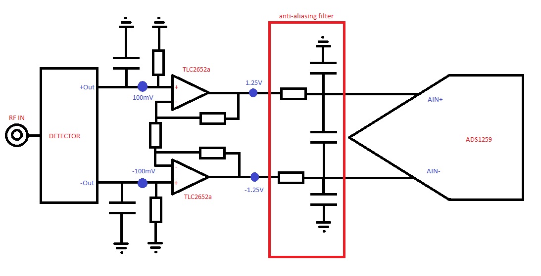
I attached a block diagram of a system I'm trying to build and I have few questions about ADS1259 .

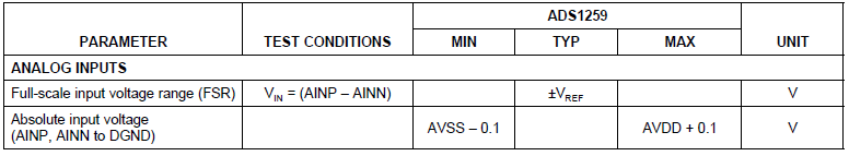
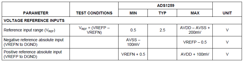
1) What is the max input voltage on ADS1259 analog input pins if I'm using +-2.5V supply and a external reference REF5025 and how to connect it on the VREFP and VREFN pins? VREFP=REF5025 output and VREFN=AVSS ?

2) Anti-aliasing filter, how to calculate R and C of the filter , FD=1/(2*pi*R*C)?  What corner frequency should my filter have if the output of DETECTOR is DC voltage?

3) In the datasheet of TLC2652a stand that Equivalent input noise voltage Vn(f=10Hz)=140nV/sqrt(Hz) and if i have gain=3 the output noise is 420nV/sqrt(Hz), and the noise of ADS1259 (Table1 in datasheet) @ 1200SPS = 2.3uVRMS and if I use 10Hz band filter that means noise after filter is =sqrt(1.57*BW)*420n=1.66uVRMS ? But i saw that the corner frequency of filter must be greater or equal FD for the 1.2kHz NOISE=18uVRMS , or I'm wrong ? How is this connected  if you can give me a hint.

Best Regards.

  • Hi David,

    Welcome to the TI E2E forums!

    I don't see your block diagram. Did you delete the text link to it after attaching it? Regarding your questions:

    1) The max and min analog input voltage on either input is limited by the supply voltages. Typically, you don't want the input signals to exceed the supply rails or you will turn on ESD diodes between the inputs and supplies. Additionally, the differential voltage between AINP and AINN (the positive and negative analog inputs) should not be greater than the reference voltage, otherwise the digital output code will saturate at full-scale. 

    The reference inputs behave similarly with absolute and differential limits. You can connect VREFN to AVSS and VREFP to AVSS + 2.5V. To do this though, the REF5025 needs to be referenced (grounded) to AVSS.


    2) I don't have the block diagram to see what you're referencing, however, if the input signal is a DC voltage you can use a low cutoff frequency. Just keep in mind that step changes (during power-up for example) will take a longer time to settle and you may have some invalid conversions results while the ADC is sampling the charging capacitor voltages.


    3) If I understand you correctly, you are calculating the RMS noise contribution of the op amp after the RC filter. You are mostly correct in your calculation, however, you need to multiply the noise density by the bandwidth squared:  420nVrms/Sqrt(Hz) * [1.57*10Hz]^2 = 103uVrms.

    This noise value will be added to the intrinsic noise of the data converter (2.3uVrms @ 1.2kSPS).  Adding non-correlated noise sources: sqrt(103uVrms^2 + 2.3uVrms^2)  = 103.55uVrms.

    You can see that the op amp noise dominates. The TLC2652 is a older device with high noise. You can find newer op amps with much lower noise, closer to 1nV/sqrt(Hz) which will give you better performance, especially when used with a 24-bit data converter. You will want the op amp noise contribution to be comparable to the ADC's intrinsic noise or much less to get the full performance of the ADC, otherwise you will not benefit from a 24-bit data converter.

    If you can share the block diagram and any op amp requirements you have for your application, I could help recommend a lower noise op amp.

    Regards,
    Chris

  • Thanks for answers, I think I attached it right this time :)

    ->You can connect VREFN to AVSS and VREFP to AVSS + 2.5V

    The pin VREFP=0V?

    ->If you can share the block diagram and any op amp requirements you have for your application, I could help recommend a lower noise op amp.

    I picked the TLC2652 because it say's that is Chopper-Stabilized referred to this "http://epic.mcmaster.ca/~elmer101/sqlaw/detcircu.html"

    Regars,

    David.

  • Hi David,

    I'm sorry, I was off on my units in my noise calculation yesterday. Your calculation is correct, you get 1.66uVrms on the output of the TLC2652 with a gain of 3. In a two op amp instrumenation amplifier configuration (like you have), the noise is further increased by sqrt(2) becuase the noise of each amplifer adds in a non-correlated way.

    I simulated the noise this time to double check that I'm not misleading you.

    4186.TLC2652 CKT.TSC


    David V said:

    The pin VREFP=0V?

    Yes! See the ADS1259EVM schematic on page 39 of this document: http://www.ti.com/lit/ug/sbau163a/sbau163a.pdf. The REF5025 is connected in this way.


    David V said:

    I picked the TLC2652 because it say's that is Chopper-Stabilized referred to this "http://epic.mcmaster.ca/~elmer101/sqlaw/detcircu.html"

    Thank you for this reference! It is correct in it's noise analysis. However, we do have much newer devices that provide the low offset and low drift drift, similar to the TLC2652, but have much lower noise and are lower power devices. Check out the OPA2333 or OPA2188 which are also dual packages.

    Regards,
    Chris

  • Thanks for the hint for ADS1259EMV schematic.

    About the OPA2333 and OPA 2188 are they also Chopper-Stabilized? ( I'm not sure the meaning but I think that means that they have low offset voltage), they have 10 times more offset than tlc2652.

    I'm trying to detect power up to -50 dBm and the min output from detector is about +-100 uV so offset and noise really matters :).

    About the anti-aliasing filter cutoff frequency and the data output rate Fd, Bonnie Baker says in "http://www.edn.com/electronics-blogs/bakers-best/4314103/Using-an-analog-filter-to-inject-noise" that "It can be as high as you want, as long as you keep in mind that your filter’s corner frequency is equal to or greater than the converter’s output-data rate." but what if it's lower , because i have a DC i like to use eg. 10 Hz filter that lowers the noise but it's  lower than the 1200 SPS = FD = 1.2 kHz?

    Or will just the Settling time incrase and what is the bad effect of this, is there a way to calculate the Settling time?

    Sorry if I have to many questions, but I'm a student and I want to learn about this things :)

    Regards,

    David.

  • Hi David,

    Yes, the OPA2333 and OPA2188 are chopper-stabilized. I'm sorry, I did not look carefully enough at the offset. I am actually really surpirsed how well the TLC2652 specifications holds up against state-of-the-art chopper-stabilied op amps. I was just trying to recommend lower noise and lower power devices that might give better performance. I would also recommend checking out the LMP2022 if you want to go down that route.

    If your cutoff frequency is below the ADC datarate your filter will reduce the noise even further. You don't need to worry as much about a maximum resistor value as the total noise will be limited by the size of the capacitor now. (kT/C noise)

    The settling time is directly related to the RC filter's time constant.

    Regards,
    Chris

  • Hi,

    I think I'm going to use 10 to 100 Hz band filter because the noise after the filter is comparable with the noise of ADS1259.

    Could you pleas suggest me what linear voltage regulator should i choose for 5V , -5V , 2.5V and -2.5V for my application and 3.3V for MSP430F5508?

    Regards.

  • Hi Chris

    How to start simulations in TINA after I open the file that you attached and change some values?

    Regards,

    David.

  • Hi David,

    From the "Analysis" menu you can run DC sweeps (Called "DC Transfer Characteristic..." in the DC Analysis sub-menu), Frequency Sweeps (Called "AC Transfer Characteristic..." in the AC Analysis sub-menu), or Noise Analysis (highlighted below).


    You can also find more documentation on Tina-TI here: http://www.tina.com/English/tina/document

    Regards,
    Chris

  • Hi Chris

    When I choose Noise Analysis a pop-up error appears

    Regards,

    David.

  • Hi David,

    There are three types of voltage inputs in TINA:

    In your circuit there are two "Voltage Generators" and both default to the "INPUT" I/O state. Therefore, TINA does not know which input to use for the noise analysis.

    You will have to test these circuits one at a time (either split them into two files or change the I/O State of one of the voltage generators to "NONE"). I had put them into one file for comparison, but I did the noise analysis separately.

    Regards,
    Chris