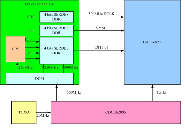
Now, I am using DAC5682Z as the follow figure show:
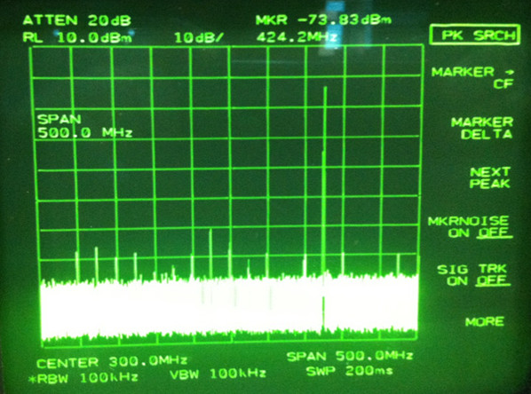
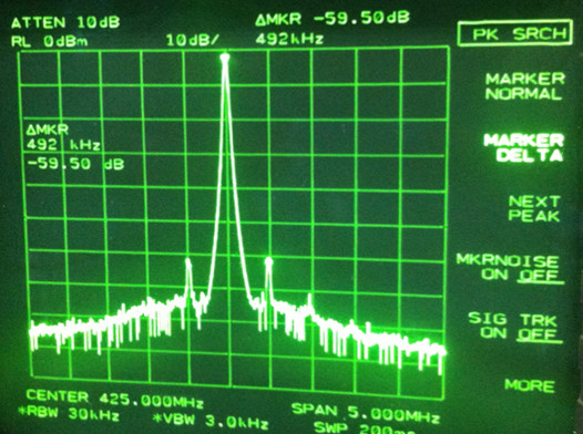
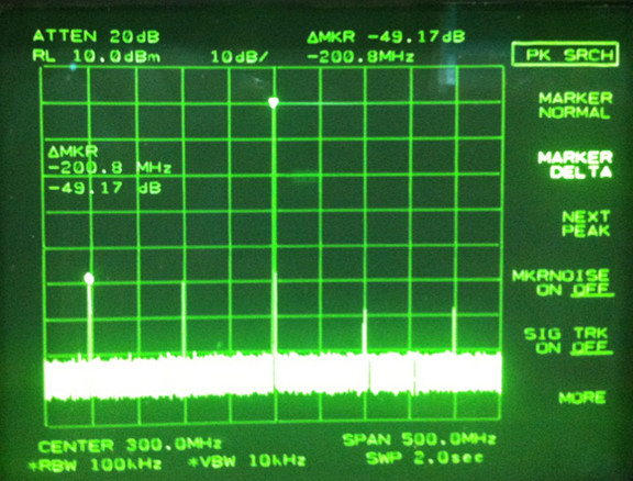
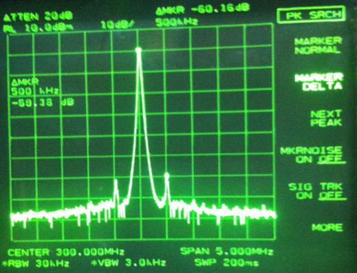
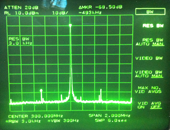
I want to generate signal between 175MHz to 425MHz, so I write a test program which generate a 425MHz signal to test the DAC5682Z.
I use CDCE62005 to generate 1GHz and 500MHz clock for DAC5682Z and FPGA.
In FPGA, I use 4 bits OSERDES to generate DDR data for the DAC5682Z.
And, I configure the DAC5682Z’s registers through SPI interface as follow:
1, Configure the CDCE62005 to generate the clocks for DAC5682Z and FPGA.
/*Provide stable clocks for DAC5682Z and FPGA */
2, Reset DAC5682Z through the RESETB pin
/* Set he DAC5682Z to initial status */
3, CONFIG8 0x07 = 0x04;
/* Set DLL restart */
4, CONFIG2 0x02 = 0x80
/*Set the DAC5682Z to single DAC mode*/
5, CONFIG1 0x01 = 0x00
/* Disable the filters */
6, CONFIG5 0x05 = 0x82
/*Set the serial interface in 4 pin mode
Bypass the PLL */
7, CONFIG10 0x0a = 0xc0
/*when DCLKP/N is between 325MHz to 500MHz, the register should be 0xc0 through datasheet.*/
8, CONFIG8 0x08 = 0x00;
9, Read the register 0 to check if the DLL is locked.
I want to generate a 425MHz signal, but the generate signal is actual 375MHz? why?