This thread has been locked.

If you have a related question, please click the "Ask a related question" button in the top right corner. The newly created question will be automatically linked to this question.

ADS1148 SPI Problem

Other Parts Discussed in Thread: ADS1148

Dear Sir:

 I try to SPI Function, I write command below.

 16      --- STATAC

400001  -- Register MUX0    Value 01

420030 -- Register MUX1   Value 30

410000 -- Register Vbias  Value 00

4a0007 -- Register IDAC0 Value 07

4b0001 -- Register IDAC1  Value 01

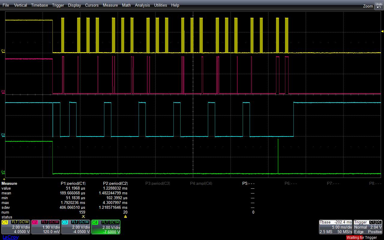
220000 -- Read Mux1 Register

FF       -- NOP  , Then Read Value is 30

FF     -- NOP

Now, I Change Value 30 to 31 of MUX1, Then I read MUX1 Value again.

The Value is not happened. It's 30.

By the way , I Change value to 34 of MUX1, The Value Change to 34.

What's happen?? Who can tell me? 

  • Hi Jordan,

    Can you send me oscilloscope or logic analyzer plots of the communication?  You need to verify that you have the correct clock/phase relationship for your communication.  The SCLK should idle low, and the phase of the data should be changing on the rising edge of SCLK and stable on the falling edge.  See Figure 1 of the datasheet.

    Best regards,

    Bob B

  • Please help me. Thank You.

  • Hi Jordan,

    The only thing I can think of is you are not communicating like you think you are, or in other words just because you can read back a value that you wrote doesn't mean it is the correct value in the ADS1148.  If you lose the LSB in your communication it is often due to incorrect communication.  The best troubleshooting tool you can use is an oscilloscope.  If you connect up a scope and take pictures of the communication, I can help you determine if the communication being sent/received is correct.

    Best regards,

    Bob B

  • Dear Bob :

    I do'nt know. The Figure is  disappear. So I post it again.

    Yellow : SCLK

    Red : SDO

    Blue : CS

    Green : SDI

    The figure is whole procedure, and the mux1 write down 0x04. I can read it in Green wave .


    figure  : The Register Mux1 write down 0x04

    Figure : The Register Mux1 write down 0x02

    Figure : Read out the Register Mux1, and can't read anything when It was wrote the value 0x02.

  • Hi Jordan,

    The good news is you are writing to the ADS1148 correctly.  The bad news is DOUT of the ADS1148 is always low.  Some things to check are making sure the RESET pin is high and START pin is high.  Also you need to make sure the device is powered correctly for both AVDD and DVDD as well as appropriate grounds.  Can you send me your schematic?

    Best regards,

    Bob B

  • Dear Bob :

     I had tried write down 0x32, but it's result was 0x30. I wrote down 0x34, and it's result was 0x34.

    I have check RESET and START signal . they are high by FPGA  control.

  • Hi Jordan,

    I don't know how you can be reading anything back as according to your scope shots the output is always zero.  Are you getting these values back from your software debugger?  Was your scope connected incorrectly?

    What I now need to see is scope shots of writing 0x32 and reading back 0x30.  Make sure you are getting data back on the DOUT pin of the ADS1148.

    Best regards,

    Bob B

  • Dear Bob :

    Write procedure

    0x16

    0x420032   -- Write the register MUX1 , It's vaule is 0x32

    0x2200     -- Read the register Mux1

    0xff       -- I can read the value is 0x30 of register Mux1.

    0xff


    Yellow : SCLK

    Red : SDO

    Blue : CS

    Green : SDI

    Figure: The whole of porcedure.

    Figure : Focused on the Mux1

    Figure : Blow up the writing Mux1

    Figure : Focused on the reading Mux1

    Figure : Blow up the reading register

    I also try the other value, 0x37, 0x3F

    Then I  read register value is 0x34, 0x3C.

    So, it is more clear bit0 and bit1 alway "0".

    I don't know! What's wrong with it?.

  • Hi Jordan,

    Thanks for scope shots.  I am confused why you are sending the extra NOP when you do the register read? 

    There are a couple of things that we need to make sure are not causing an issue.  First of all, you cannot effectively communicate to the ADS1148 until after 2^16 system clock cycles after power up.  Another consideration is SDATAC will not take effect until after the next DRDY asserts.  So when you issue the SDATAC you should wait for one conversion cycle to complete as the result will be posted automatically to the output register until SDATAC has taken effect.  When you issue SDATAC then immediately start communicating, there is no guarantee that the next update will not occur in the middle of your register read.  This will corrupt the results of the read.  The third thing to remember is START must be high to read or write the control registers.  If START is low, then the ADS1148 is in a power down state.

    Best regards,

    Bob B

  • Dear Bob :

    Unfortunately, I still can not resolve my problem. 

    You can review my waveform of the figure below.

    First, I pushed the reset button, then "DRDY "  did not fall down until 200ms.

    2nd, the controller sensed "DRDY" from low to high then to low. The controller 

             send command SDATAC. You can review figure below.

    3rd,  The controller continued sensing "DRDY"  to low, then it executed to write and read the register.

    I don't know what problem my procedure has? Please tell me.

    Sorry! my English is pool. I hope you can understand it.

             Best Regards

                                    Jordan

  • Hi Jordan,

    Unfortunately I can't tell you what is going wrong.  I can't really tell for sure that the edges are correct, but they appear to be ok.  I set this up myself and I'm able to get the expected response.

    Have you tried writing and reading to other registers?  Do you get the proper response?  Have you tried writing and reading from a block (or group) of registers to see if you get a different result?

    Best regards,

    Bob B

  • Dear Bob :

     I have sloved my problem. It has a gitch inside the SCLK.

    Now, my project need four sensors of PT100.

    Does it  procedure cprrect ??

    Step1.  SDATAC  .   => Does it  need to write command for every time if we want to change to another channel ??

    Step2. Wait DRDY is "Low"

    Step3.  Write another channel of the MUX0.

    Step4. Wait DRDY is "Low"

    Step5. RDATAC

    Step6. Wait DRDY is "Low"

    Step7. Read A/D Data

    Step8. Repeat Step1

       Best Regards,

                        Jordan

  • Hi Jordan,

    If you are using RDATAC mode, all you have to do is wait for DRDY to go low, and change the MUX at the same time as you read the data. Instead of sending NOP when you read the data you would issue a WREG command and the MUX0 data. 

    You would send 0x40, 0x00, new value of MUX0.  The next conversion will be the new MUX setting.  The first two bytes returned will be the previous conversion results.

    Best regards,

    Bob B

  • Dear Bob :

     Do I also need WREG command and the IDAC1 for the other channel ?

         Best regards

                         jordan

  • Hi Jordan,

    The first group would be WREG 0x00, 0x03 and the second group would be WREG 0x0A, 0x04 (or for how many actual registers you wish to write.)

    Best regards,

    Bob B