


hello everyone.
i have problem receiving data from ADS1291.
because of the data i get from ADS1291 is weird. so i check the first 24 bits which are status register.
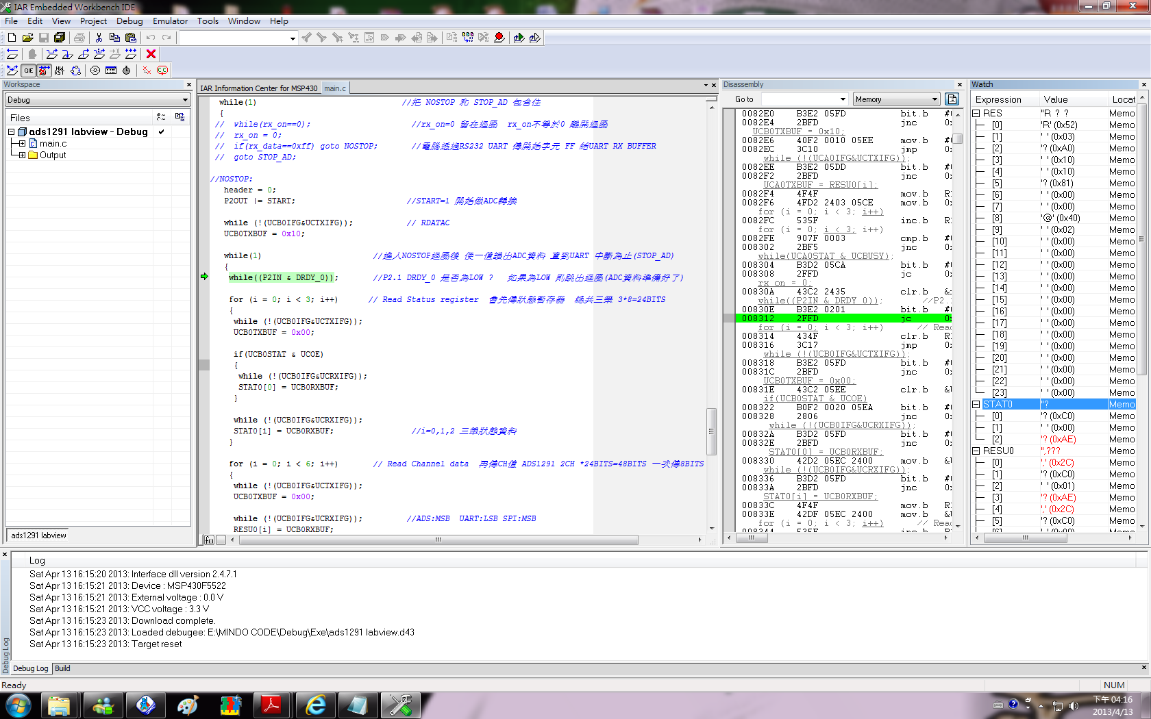
i save the Status registers in STAT[0] to STAT[2]
the status register supposed to be 0XC0 0X00 0X00
but i got wrong data.
and save the output two channel data in RESU0[0] to RESU0[5]
but i alraedy power down CH2. but still get reading from RESU0[3] to RESU0[5]
anyone can help me?
and also here is my MSP430F5522 Firmware to retreving data from ADS1291
#include <msp430f5529.h>
#include <math.h>


#define   START            0x80         // P2.7
#define   PWDN             0xFE         // P2.0
#define   RESET_BT         0xBF         // P2.6
#define   DRDY_0           0x02         // P2.1
#define   CS_0             0xEF         // P4.4


char STAT0[3], RESU0[24], STAT1[3], RESU1[24], RES[24];
char LOFF_P0, LOFF_N0, LOFF_P1, LOFF_N1, header, rx_data, rx_on=0, tx_on=0;


void configure_uart(void)
{
  P3SEL |= BIT3 + BIT4;                     // P3.3,4 = USCI_A0 TXD/RXD
  UCA0CTL1 |= UCSWRST;                      // **Put state machine in reset**
  UCA0CTL1 |= UCSSEL_2;                     // SMCLK
  UCA0BR0 = 0x08;                           // 8MMHz 921600 (see User's Guide)
  UCA0BR1 = 0x00;                           // 8MMHz 921600
  UCA0MCTL |= UCBRS_6 + UCBRF_8;            // Modulation UCBRSx=1, UCBRFx=0
  UCA0CTL1 &= ~UCSWRST;                     // **Initialize USCI state machine**
  UCA0IE |= UCRXIE;                         // Enable USCI_A0 RX inter
}


void configure_spi(void)                    //�b�o��]�wport4(�Ѧh�u��) P4DIR P4OUT
{
                                            // P1DIR |= 0x80  P1.7 for RESET_ADS
  P2DIR |= 0XC1;                            // P2.0, 6, 7 for PWDN, RESET_BT, START
  P3SEL |= BIT0 + BIT1 + BIT2;              // P3.0, 1, 2 SPI option select
  P4DIR |= 0X1F;                            // P2OUT |= ~CS_0 + ~CS_1
                                            // P4.0, 1, 2, 3, 4 for A0, A1, A2, A3, E*
  P4OUT |= ~CS_0 ;                          // Disable CS   �Ѧh�u�� E* = 1  Y0 - Y15 =1

  UCB0CTL1 |= UCSWRST;                      // **Put state machine in reset**
  UCB0CTL0 |= UCMST+UCSYNC+UCMSB;           // 3-pin, 8-bit SPI master, MSB
  UCB0CTL1 |= UCSSEL_2;                     // SMCLK
  UCB0BR0 = 0x02;                           // /2   8.192/2 =4.096 ���� 4.096 = 2*2.048
  UCB0BR1 = 0x00;                           //
  UCB0CTL1 &= ~UCSWRST;                     // **Initialize USCI state machine*
}


void main(void)
{
  char i;

  WDTCTL = WDTPW + WDTHOLD;                 // Stop WDT


  P5SEL |= BIT2+BIT3;                       // Port select XT2

  UCSCTL6 &= ~XT2OFF;                       // Enable XT2
  UCSCTL3 |= SELREF_2;                      // FLLref = REFO
                                            // Since LFXT1 is not used,
                                            // sourcing FLL with LFXT1 can cause
                                            // XT1OFFG flag to set
  UCSCTL4 |= SELA_2;                        // ACLK=REFO,SMCLK=DCO,MCLK=DCO

  // Loop until XT1,XT2 & DCO stabilizes - in this case loop until XT2 settles
  do
  {
    UCSCTL7 &= ~(XT2OFFG + XT1LFOFFG + DCOFFG);
                                            // Clear XT2,XT1,DCO fault flags
    SFRIFG1 &= ~OFIFG;                      // Clear fault flags
  }while (SFRIFG1&OFIFG);                   // Test oscillator fault flag

  UCSCTL6 &= ~XT2DRIVE0;                    // Decrease XT2 Drive according to
                                            // expected frequency
  UCSCTL4 |= SELS_5 + SELM_5;               // SMCLK=MCLK=XT2


  configure_uart();
  configure_spi();                      // Setup SPI

  P2OUT &= PWDN;                           //PWDN = 0
  P2OUT &= RESET_BT;                     // P2.6  RESET_BT
  P2OUT &= ~START;                         //START = 0
  P2OUT |= ~PWDN;                          //PWDN = 1
                                           //P2OUT |= ~CLKSEL;             // CLKSEL Pin =1 (����������512KHZ)

  P4OUT &= CS_0;                        // CS=0 CS Enable

  while (!(UCB0IFG&UCTXIFG));            // SDATAC
  UCB0TXBUF = 0x11;


  while (!(UCB0IFG & UCTXIFG)); // RREG starting at address 0  00100001  00h �}�lŪ
UCB0TXBUF = 0x20;

while (!(UCB0IFG & UCTXIFG)); // Ū1��  Registers
UCB0TXBUF = 0x00;
while (!(UCB0IFG & UCTXIFG)); // first dummy data
UCB0TXBUF = 0x00;
while (!(UCB0IFG & UCTXIFG)); // another dummy data
UCB0TXBUF = 0x00;
while (!(UCB0IFG & UCRXIFG));
RES[0] = UCB0RXBUF;


  while (!(UCB0IFG&UCTXIFG));             //�q01h�}�l�g
  UCB0TXBUF = 0x41;

  for (i = 0; i < 10; i++);

  while (!(UCB0IFG&UCTXIFG));             //�g1�ӼȦs��
  UCB0TXBUF = 0x00;

  for (i = 0; i < 10; i++);

  while (!(UCB0IFG&UCTXIFG));       // WREG CONFIG1 0x03   00000011  continuous mode, Data rate = 1KSPS
  UCB0TXBUF = 0x03;

  for (i = 0; i < 10; i++);


  while (!(UCB0IFG&UCTXIFG));             //�q09h�}�l�g
  UCB0TXBUF = 0x49;

  for (i = 0; i < 10; i++);

  while (!(UCB0IFG&UCTXIFG));             //�g1�ӼȦs��
  UCB0TXBUF = 0x00;

  for (i = 0; i < 10; i++);

  while (!(UCB0IFG&UCTXIFG));       // WREG RESP1 0x02   00000010
  UCB0TXBUF = 0x02;

  for (i = 0; i < 10; i++);


  while (!(UCB0IFG&UCTXIFG));             //�q02h�}�l�g
  UCB0TXBUF = 0x42;

  for (i = 0; i < 10; i++);

  while (!(UCB0IFG&UCTXIFG));             //�g2�ӼȦs��
  UCB0TXBUF = 0x01;

  for (i = 0; i < 10; i++);


  while (!(UCB0IFG&UCTXIFG));             // WREG CONFIG2 0xA0   10100000  internal reference 2.4 V
  UCB0TXBUF = 0xA0;

  while (!(UCB0IFG&UCTXIFG));             // WREG Lead-Off Control Register 0x10   00010000
  UCB0TXBUF = 0x10;

  while (!(UCB0IFG&UCTXIFG));            //�q04h�}�l�g
  UCB0TXBUF = 0x44;

  while (!(UCB0IFG&UCTXIFG));            //�g��ӼȦs��
  UCB0TXBUF = 0x01;

  while (!(UCB0IFG&UCTXIFG));             // WREG CH1     0x10   00010000
  UCB0TXBUF = 0x10;

  while (!(UCB0IFG&UCTXIFG));             // WREG CH2     0x81   10000001   power down CH2
  UCB0TXBUF = 0x81;

  while (!(UCB0IFG&UCTXIFG));             //�q08h�}�l�g
  UCB0TXBUF = 0x48;

  while (!(UCB0IFG&UCTXIFG));            //�g�@�ӼȦs��
  UCB0TXBUF = 0x00;

  while (!(UCB0IFG&UCTXIFG));            //    01000000   CLK_DIV = 1 , CLK = 2.048MHZ
  UCB0TXBUF = 0x40;

  while(UCB0STAT & UCBUSY);

 while (!(UCB0IFG & UCTXIFG)); // RREG starting at address 1  00100001  01h �}�lŪ
UCB0TXBUF = 0x21;

while (!(UCB0IFG & UCTXIFG)); // Ū9��  Registers
UCB0TXBUF = 0x08;
while (!(UCB0IFG & UCTXIFG)); // first dummy data
UCB0TXBUF = 0x00;
while (!(UCB0IFG & UCTXIFG)); // another dummy data
UCB0TXBUF = 0x00;
while (!(UCB0IFG & UCRXIFG));
RES[1] = UCB0RXBUF;
while (!(UCB0IFG & UCTXIFG));
UCB0TXBUF = 0x00;
while (!(UCB0IFG & UCRXIFG));
RES[2] = UCB0RXBUF;
while (!(UCB0IFG & UCTXIFG));
UCB0TXBUF = 0x00;
while (!(UCB0IFG & UCRXIFG));
RES[3] = UCB0RXBUF;
while (!(UCB0IFG & UCTXIFG));
UCB0TXBUF = 0x00;
while (!(UCB0IFG & UCRXIFG));
RES[4] = UCB0RXBUF;
while (!(UCB0IFG & UCTXIFG));
UCB0TXBUF = 0x00;
while (!(UCB0IFG & UCRXIFG));
RES[5] = UCB0RXBUF;
while (!(UCB0IFG & UCTXIFG));
UCB0TXBUF = 0x00;
while (!(UCB0IFG & UCRXIFG));
RES[6] = UCB0RXBUF;
while (!(UCB0IFG & UCTXIFG));
UCB0TXBUF = 0x00;
while (!(UCB0IFG & UCRXIFG));
RES[7] = UCB0RXBUF;
while (!(UCB0IFG & UCTXIFG));
UCB0TXBUF = 0x00;
while (!(UCB0IFG & UCRXIFG));
RES[8] = UCB0RXBUF;
UCB0TXBUF = 0x00;
while (!(UCB0IFG & UCRXIFG));
RES[9] = UCB0RXBUF;


  while(UCB0STAT & UCBUSY);           //SPI �p�GUCBUSY=0 ���m  �p�GUCBUSY=1 USCI ���b�����ζǿ�


  _EINT();

  P2OUT |= ~RESET_BT;

  while(1)                              //�� NOSTOP �M STOP_AD �]�t��
  {
   while(rx_on==0);                     //rx_on=0 �d�b�j��  rx_on������0 ���}�j��
   rx_on = 0;
   if(rx_data==0xff) goto NOSTOP;       //�q���z�LRS232 UART �Ƕ}�l�r�� FF ��UART RX BUFFER
   goto STOP_AD;

NOSTOP:
   header = 0;
   P2OUT |= START;                       //START=1 �}�l��ADC�ഫ

   while (!(UCB0IFG&UCTXIFG));           // RDATAC
   UCB0TXBUF = 0x10;

   while(1)                       //�i�JNOSTOP�j��� �K�@��Ū�XADC��� ����UART ���_����(STOP_AD)
   {
    while((P2IN & DRDY_0));       //P2.1 DRDY_0 �O�_��LOW ?   �p�G��LOW �h���X�j��(ADC��ƷdzƦn�F)

    for (i = 0; i < 3; i++)      // Read Status register  �|���Ǫ��A�Ȧs��  �`�@�T�� 3*8=24BITS
    {
     while (!(UCB0IFG&UCTXIFG));
     UCB0TXBUF = 0x00;

     if(UCB0STAT & UCOE)
     {
      while (!(UCB0IFG&UCRXIFG));
      STAT0[0] = UCB0RXBUF;
     }

     while (!(UCB0IFG&UCRXIFG));
     STAT0[i] = UCB0RXBUF;                //i=0,1,2 �T�����A���
    }

    for (i = 0; i < 6; i++)       // Read Channel data  �A��CH�� ADS1291 2CH *24BITS=48BITS �@����8BITS
    {
     while (!(UCB0IFG&UCTXIFG));
     UCB0TXBUF = 0x00;

     while (!(UCB0IFG&UCRXIFG));         //ADS:MSB  UART:LSB SPI:MSB
     RESU0[i] = UCB0RXBUF;
    }

    RESU0[2]=RESU0[2] & 0xFE;            // RESU0[2]�s�Ĥ@��CH �� 7-0 ��BIT?  &  11111110
    RESU0[2]=RESU0[2] | header;          // �o��ݤ����� ���ƻ�n & 0xFE? | header? header �@�άO?
    header++;                      //BIT0 =0,1,0,1,0,1    �O�_��UART�ǿ�?(�_�l0 ����1) 1-0 �}�l�ǰe
    if ( header == 2 ) header = 0;

    for (i = 0; i < 3; i++)              // Send Channel data to BT  �Ǥ@��CH��DATA  �u����CH1 DATA
    {
     while (!(UCA0IFG&UCTXIFG));         // USCI_A0 TX buffer ready?
     UCA0TXBUF = RESU0[i];               // i=0,1,2
     if(rx_on>0 && rx_data==0x00) goto STOP_AD;    //�p�G�o��UART���_ �R�O����ADC���� �hrx_on�j��0 �B rx_data=0x00
    }
    while(UCA0STAT & UCBUSY);
    rx_on = 0;
   }                                              //�~�� NOSTOP While(1) �j��
STOP_AD:
   rx_on = 0;
  }

}

#pragma vector=USCI_A0_VECTOR
__interrupt void USCI_A0_ISR(void)    //P997 UART ���_   �q�Q�O�q���z�LRS232 UART�Ǹ�Ƶ�RX Buffer �y��RX���_
{
   rx_data = UCA0RXBUF;               //UART �ϥ� FF��@�}�l�r��  00��@����r��
   rx_on++;
}

