This thread has been locked.

If you have a related question, please click the "Ask a related question" button in the top right corner. The newly created question will be automatically linked to this question.

SPI interface of lmp90100 with arduino...

Other Parts Discussed in Thread: LMP90100, ADS1248, LMP91300

he TI..

glad to know about this perfect AFE for sensor...i want to use this one in my application but i am lilll confused in using it. my first confusion is 

how i programe the internal registers.please make me understand in a programming aspect as i m a beginner in SPI communication...

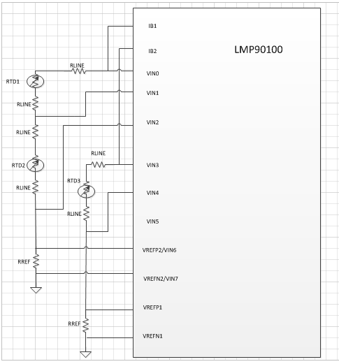
can i use 3 RTD in 4 wire configuration connected in series with same current source and same Rref as only one RTD voltage is sampled at a time. if this not possible then how can i connect 3 RTD in 4 wire configuration with a single LMP90100.

please suggest me any application note wich can describe SPI communication in contrast to this IC.

  • Varun,

    A good SPI programming reference would the following App Note:

    http://www.ti.com/general/docs/lit/getliterature.tsp?literatureNumber=snaa134a&fileType=pdf

    Source code can be found in the LMP90100 product folder in the Software section: http://www.ti.com/product/LMP90100

    All 4 wires of 3 RTD would be a difficult connection. See following schematic where you could use the 4 wire RTD's as 2 wire RTD's.

    Also consider the ADS1248

  • Hi,
    Is there any arduino code available ?
    Ayanga
  • Hello Ayanga,

    On the LMP90100 web page, click on the Tools & Software tab. There is a file called "MSP430 Interface to LMP90100 Code Library" (snac029) that has some the C code for some demos. You can use these as examples as a starting point for your project.

    Mike
  • Dear Mike,
    Thanks alot for the help. But it looks more like from MSP 430 point of view. I am not familiar with this IC. I would like to know SPI specifications required for LMP90100?
    Ayanga
  • Hi Mike,
    I prepared an arduino code according to demo-app01. But it returns value 512 all the time as reg_read _data though reg_write_data is 86.
    I changed reg_write_data to another value but it still gives 512 as the reg_read _data . My arduino code is bellow.
    #include <SPI.h>
    const int chipSelectPin = 42;
    void setup() {
    int prev_URA; // Previous Upper Register Address (URA)
    int reg_write_data, reg_read_data;

    Serial.begin(9600);
    // start the SPI library:
    SPI.begin();
    // initalize the data ready and chip select pins:
    pinMode(chipSelectPin, OUTPUT);

    prev_URA =0XFF;
    reg_write_data = 0x56;
    TI_LMP90100_SPIWriteReg(0x11, reg_write_data,&prev_URA);
    reg_read_data = TI_LMP90100_SPIReadReg(0x11,&prev_URA);
    Serial.println("Write_data");
    Serial.println(reg_write_data);
    Serial.println(reg_read_data);

    }

    void loop() {
    // int reg_write_data, reg_read_data;
    // int prev_URA;
    // prev_URA =0XFF;
    // reg_read_data = TI_LMP90100_SPIReadReg(0x11,&prev_URA);
    // if (reg_read_data)
    // Serial.println(reg_read_data);

    // put your main code here, to run repeatedly:

    }


    void TI_LMP90100_SPIWriteReg(int addr, int value, int *pURA)
    {
    int new_URA, inst;

    new_URA = (addr & 0x70)>>4; // extract upper register address
    Serial.println("SpiWrite");
    digitalWrite(chipSelectPin, LOW);
    if (*pURA != new_URA) // if new and previous URA not same, add transaction 1
    {
    inst = 0x10;
    SPI.transfer(inst);
    delay(10);
    SPI.transfer(new_URA);
    delay(10);
    *pURA = new_URA;
    }
    inst = 0x00 | 0x00 |(addr & 0x0F); // lower register address
    SPI.transfer(inst);
    delay(10);
    SPI.transfer(value);
    delay(10);
    digitalWrite(chipSelectPin, HIGH);
    }

    int TI_LMP90100_SPIReadReg(int addr, int *pURA)
    {
    int x, new_URA, inst;

    new_URA = (addr & 0x70)>>4; // extract upper register address
    digitalWrite(chipSelectPin, LOW);
    if (*pURA != new_URA) // if new and previous URA not same, add transaction 1
    {
    inst = 0x10;
    SPI.transfer(inst);
    delay(10);
    SPI.transfer(new_URA);
    delay(10);
    *pURA = new_URA;
    }
    inst = 0x80 |0x00 | (addr & 0x0F);
    SPI.transfer(inst);
    delay(10);
    inst=0x00;
    while(!x)
    x=SPI.transfer(inst);
    delay(100);
    Serial.println("SpiRead");
    Serial.println(x);
    delay(100);
    digitalWrite(chipSelectPin, HIGH);
    return x;
    }
  • Hello Ayanga,

    In answer to your question the LMP91300 follows normal SPI protocols. The timing requirement s are listed in the datasheet.

    With regards to your code, have you been able to look at the SPI signals and make sure that the correct signals are going to the LMP90100?

    Since I am not familiar with Arduino coding and can't give you much help there, another thought is to try code to do the Quick Start listed in the datasheet. This will at least give you a result as to whether the code is correct.

    Mike
  • Hi Varun,
    Me to has the same problem. Have you found any solution?
    Ayanga
  • Hi Mike,
    Can you tell me whether I can use SPI Probe (J8) to program internal registers without using SPIO-4 board and LMP90100 software?
    Ayanga
  • Hello,

    Yes, you can connect your SPI signals directly to J8.

    Mike
  • Hi Mike,

    I checked the signals with a logic analyzer. SCK, CS and MOSI ,MISO are accurate. What do you mean by timing requirements ? can you explain a bit. I set SPI MODE 1 as data mode.

    Ayanga 

  • Hello Ayanga,

    The timing requirements are shown starting on page 11 of the datasheet. They describe the relationship of the edges and hold times of the CSB, SCLK, SDI and SDO signals. If the Arduino uses standard SPI it should be ok. I am not sure what mode is the correct one, you will need to check your waveforms with the drawings in the datasheet.

    Also check that you are doing the addressing correctly as describe in section 9.5. The URA and LRA scheme is unique.

    Mike
  • Hi Mike,
    Thanks a lot for your continuous help !!! There was a timing issue due to a silly mistake of mine. (Insert delay between 8-bit spi transactions )
    It works well now .
    Ayanga
  • Dear Jason,

    I have the same question as Varun and did'nt quite get the answer. Is it possible to use a single Rref alone across only  VREFP2 - VREFN2 ? For example you have used only a single Rbias across REFP0 and REFN0 to measure from all the three RTD's on the ADS1248. Can the same configuration not be used with lmp90100.

    Thanks,

    Sathish

  • Hi Satish,

    The limiter is the number of current sources you have. The LMP90100 has 2 current sources. If you use the topology shown in Figure 80 in the datasheet you can use 2 RTDs. The first RTD would use IB1, VIN0, VIN1, VREFP2, and VREFN2. The second RTD could use IB2, VIN2, VIN3, VREFP1, and VREFN1. It would be harder to use the same resistor across one set of VREF pin, because both current sources turn on at the same time, so you would have the currents of both RTDs going through RREF at the same time.

    Mike
  • Thanks Mike.

    Can I also connect two RTDs(both 2 wire and 3 wire RTDs) with the topology shown in Figure 78, which uses two current source per RTD. 

    Also, can I omit the compensation resistance RCOMP without much impact on the accuracy ?

    Thanks,

    Sathish

  • Hi Sathish,


    If you are using the topology in Figure 78 you can only connect one RTD.  You would need another two current sources to be able to connect another RTD.  Another possibility is to use a device to switch to connect the current sources to one or the other of the RTDs, if you want to use two of them in the Figure 78 topology.

    Yes, you can leave RCOMP out.  It is used to set the Vin to be0V at any temperature.

    Mike

  • Hello Ayanga,

    i am also using LMP90100 and trying write the value to register of LMP90100 and reading the value written to the register using arduino, but i am getting different output (not getting the same value written to the register),

    this is my code

    #include <SPI.h>
    void setup()
    {
    Serial.begin(9600);
    }

    void loop()
    {
    digitalWrite(SS, HIGH);

    SPI.begin();
    SPI.beginTransaction(SPISettings(893000, MSBFIRST, SPI_MODE1));
    //writing the value at register 0x21
    digitalWrite(SS, LOW);
    SPI.transfer(0x10); //inst 1
    delay(100);
    SPI.transfer(0x02); // ura setup
    delay(100);
    SPI.transfer(0x01);// lra setup
    delay(100);
    SPI.transfer(0x33); // value
    delay(100);
    digitalWrite(SS, HIGH);
    //reading value at register 0x21
    digitalWrite(SS, LOW);
    SPI.transfer(0x10);//inst 1
    delay(100);
    SPI.transfer(0x02); // ura setup
    delay(100);
    SPI.transfer(0x81);// lra setup
    delay(100);
    byte reg = SPI.transfer(0x00); // reading value
    delay(100);
    digitalWrite(SS, HIGH);

    SPI.endTransaction();
    SPI.end();
    Serial.println(reg, HEX);
    delay(100);
    }
    suggest me where i am going wrong.

    Charanraj
  • Hello Charanraj,

    Start off by checking that all connections are being properly made to the LMP90100. Do you have power and ground at the pins of the part? Check right at the part. Are your SPI signals also present at the pins of the part? Check your SPI signals with an oscilloscope. Do they match Figure 1 in the datasheet? Are all the timing specifications being met? What data do you see on the SDO pin when you send your write and read sequence?

    Mike
  • Hi Ayanga,

    how much delay you have used between 8-bit spi transactions. and which SPI mode you have used.

    charanraj