This thread has been locked.

If you have a related question, please click the "Ask a related question" button in the top right corner. The newly created question will be automatically linked to this question.

DAC3482EVM configuration issue using EVM GUI (App controls in a "stuck" state)

Other Parts Discussed in Thread: CDCE62005, DAC3482, ADS4249

Hi,

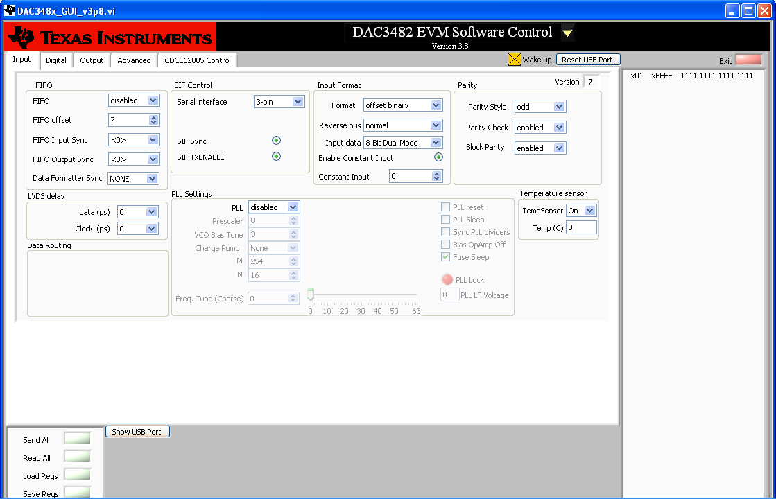
I am using a DAC3482EVM with the version 3.8 EVM GUI.  I have setup a configuration file for the DAC3482 & CDCE62005 from the EVM GUI and have loaded it into the EVM.  The GUI is running and I can make adjustments to the CDCE62005 and see changes in the EVM HW as desired.  The control screens of the DAC3482 appear to be in a predisposed state.  This DAC setup is not what I want.  When I attempt to make adjustments to any of the DAC control registers from the GUI fields the App just switches them back.  And the App has not specifically loaded the registers I originally saved.

Originally I defined settings within the DAC GUI with the DAC physically powered off and saved those settings in a file (see below).  When I load those settings with the DAC EVM powered on the GUI controls are stuck in this undesired state.  What am I doing wrong?

Thanks in advance for advise on this issue.

Pete

   x00	   xF10A
   x01	   x0000
   x02	   x8002
   x03	   xA000
   x04	   xFFFF
   x05	   x0A60
   x06	   x2C00
   x07	   xFFFF
   x08	   x0000
   x09	   x8000
   x0A	   x0000
   x0B	   x0000
   x0C	   x05A6
   x0D	   x05A6
   x0E	   x05A6
   x0F	   x05A6
   x10	   x3000
   x11	   x0000
   x12	   x0000
   x13	   x0000
   x14	   x0000
   x15	   x0000
   x16	   x3333
   x17	   x3333
   x18	   x205F
   x19	   x10F4
   x1A	   x4820
   x1B	   x0800
   x1C	   x0000
   x1D	   x0000
   x1E	   x1118
   x1F	   x8886
   x20	   x4100
   x22	   x1B1B
   x23	   x001F
   x24	   x1000
   x25	   x7A7A
   x26	   xB6B6
   x27	   xEAEA
   x28	   x4545
   x29	   x1A1A
   x2A	   x1616
   x2B	   xAAAA
   x2C	   xC6C6
   x2D	   x0000
   x2E	   x0000
   x2F	   x0000
   x30	   x61A8
   x7F	   x0004
CDCE62005 Registers
Freq:19.200000MHz
Address	Data
00		80400020
01		801C0301
02		C1800302
03		C1840303
04		81400304
05		281C1A55
06		04BF09E6
07		151877F7
08		20001C08

  • Hi Pete,

    I have loaded your setup onto the EVM and the setting is different than your picture above. I see FIFO input sync set to "None" and FIFO output and data formatter set to "SYNC". The setting did not make much sense in terms of actual application setup, but I suspect that you saved this in the middle of debugging.

    You may want to check if there are other USB devices that could cause conflict with our on-board FTDI245RL USB to serial output chip. Please unplug other devices if possible and leave only the DAC3482EVM connected to the PC before trying again.

    Also, we have seen the 1.2VDIG rail on the EVM have some oscillations on the rail due to dust or flux residue. Could you double check the 1.2VDIG rail with the multimeter to see if the voltage is correct? If not, we may need to check if there are flux residue or dust collection near the 1.2VDIG rail supply, and clean the area up accordingly. 

    -KH

  • Kang,

    Thanks for the feedback.  I have made some progress, but still have 1 main question.  I was having a little trouble getting the DAC3482 chip to talk through the serial interface and this was a wiring issue on the EVM.  I have resolved that now and I am successfully programming both the CDCE62005 & the DAC3482 via a serial interface I have instantiated through an FPGA.  I am attempting to get the HW setup TI has described as "Interfacing Altera FPGAs to ADS4249 and DAC3482" (document SLAA545) running with an Altera FPGA [ ADC --> FPGA --> DAC ].  The documentation and FPGA source code TI has provided has been helpful.  There is one aspect of the signal interface I still do not understand though.  TI provides three documents on this topic

    - "Interfacing Altera FPGAs to ADS4249 and DAC3482" pdf document

    - Altera QAR file that offers FPGA source code providing a "pass through" clock - bus system from ADC - to - DAC (ads4249_dac3482_interfaces.qar)

    - example configuration files for the DAC3482EVM [DAC + CDCE] (TI_CDCE62005_PLL_Configuration_ADC-FPGA-DAC.zip)

    My question is related to your review of the DAC FIFO synchronization method I first suggested.  The example chip config file (TI_CDCE62005_PLL_Configuration_ADC-FPGA-DAC.zip) utilizes the DAC FRAME signal to sync the DAC FIFO's input side & the input logic Data Formater.  But, the FPGA source code only provides "sync" configured as an FPGA output signal to the DAC.  How should I connect this to the DAC to support DAC synchronization?  The DAC3482EVM diff signal pair named "FIFIO-ISTR" is routed to FPGA input pins, not output; so I am thinking this signal must be for the TI TSW product instead.  Should I route this "sync" signal for the DAC FIFO input side to the SYNC HW signal or to the FRAME HW signal?  It is exactly how to synchronize the DAC FIFO with the FPGA source code that has me confused.

    I understand this signal (sync) will align the DAC input FIFO to a DATACLK edge and the OSTR signal (from the CDCE62005 system clock source) will align the DAC output FIFO with DACCLK.

    Any insight on this would be helpful.

    Thanks,

    Pete

  • Pete,

    The FIFO and clock divider can be programmed to listen to either the rising edge of FRAME or rising edge of SYNC. In terms of synchronizing the FIFO and clock divider, there are no differences between the two signals. The design team leaves the options to the user in case there are some PCB routing advantages when choosing the signals. In your case, you should map this to a valid FPGA output connecting either to FRAME or SYNC instead, and make sure the DAC GUI has the corresponding setting.

    The SYNC signal does provide additional functionality in terms of synchronization multiple DAC chip's on-chip PLLs. If your application requires synchronizing multiple devices with on-chip PLL enabled, then you will need to make sure that the SYNC signal is routed accordingly.

    -KH

  • Kang,

    Thanks for your help with this.  I have been able to properly configure the following setup:

    ADS62P49EVM --> TI_TSW-to-HSMC_bridge --> Altera_S.IV_GX530N_FPGA --> DAC3482EVM

    and pass analog signals from end-to-end using the digital loopback function described in the TI writeup "Interfacing Altera FPGAs to ADS4249 and DAC3482".  My setup utilizes a DAC3482EVM with a HSMC digital bus connector.

    Pete