This thread has been locked.

If you have a related question, please click the "Ask a related question" button in the top right corner. The newly created question will be automatically linked to this question.

Output of DAC3152

Other Parts Discussed in Thread: DAC3152EVM, DAC3152, CDCP1803

Hi,

Just starting with basic, I am trying to generate a simple square with DAC3152EVM through TSW1400.

I am giving a data of "0000000000" and "1111111111" alternately after every 250 us.

Instead of seeing a proper square wave at transformer output, what I am seeing is...

For: "0000000000" => o/p is 400mV and then exponentially decreasing to 0 mV.

       "11111111111" => o/p is -400mV and then exponentially increasing to 0 mV.

The o/p is at +ve or -ve peak during change of input only but after it o/p is drifting towards 0mV even though inputs are constant..

I tried by giving constant 0's OR 1's,  in both cases the o/p is 0mV but datasheet says => An offset binary data pattern of 0x000 at the DAC input results in a full-scale current sink and the least-positive voltage on the IOUTAP pin. Similarly, a 0x3FF data input results in a 0-mA current sink and the most-positive voltage on the IOUTAP pin.

Please let me know if I am missing something while handling a DAC3152.

Prashant


  • Prashant,

    The output transformer on the DAC3152 has a minimum input frequency of 300KHz. You are operating at 4KHz. You are just seeing the effects of the transformer, which is acting like an inductor at this low data rate. Try increasing your date rate to at least 1MHz to get a valid square wave from this evm. If you must operate at such a low data rate, you will need to remove the transformer or find one with a lower input bandwidth.

    Regards,

    Jim  

  • Hi Jim,

    Thanks For Reply !!

    I have tried with data rate of 1.13 MHz, in this case also I unable to get proper square wave.

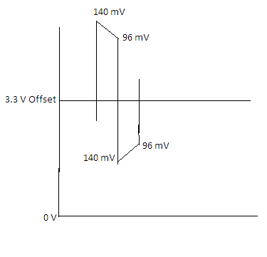
    As I mentioned earlier, when o/p is supposed to be at high voltage level, it is decreasing till half cycle. Please refer below image.                   

    If I give All zeros/ones to DAC input, what would be the o/p of DAC and Transformer.

    Prashant

  • Attaching the image file !!!!Both DAC IOUT-P and transformer output are replicated in figure.

  • Hi Prashant,

    The transformer cannot pass DC signals. So if you apply a constant signal then you'll see 0V at the transformer output, no matter what DC level the DAC is outputting. If you apply a slow square wave, you'll see the flat part of the square wave decay exponentially because the transformer cannot pass the low frequency signal. What you're seeing is expected. If you generate a faster square wave that is within the passband of the transformer then you will not see the signal decay.

    The transformer datasheet is here:

    http://www.minicircuits.com/pdfs/ADTT1-1.pdf

    Regards,
    Matt Guibord 

  • Hi Matt,

    I may not be able to see the transformer output as I expected, but I thought I can see expected waveform at transformer input OR DAC output

    But transformer input also has same behaviour.

    Attaching image file ( Opps !! where are these image files going which I have attached in previous replies ???)


    Prashant


  • Hi Prashant,

    Also note that the clock input stage has AC coupling in the DAC3152 EVM as a standard configuration. The LVPECL clock is provided with AC Coupling to DAC Clock pins DCLKP and DCLKN from CDCP1803.

    If you are running the DAC at very low speeds, say, lesser than 1MHz, you will find the significant loss of the clock input to the DAC.  Please monitor the clock input voltage at DCLKP/N and the differential voltage needs to be at least 200mV for the DAC operation.

    You can use the single ended configuration for the clocking, if you intend to use this DAC at very low speeds. You can refer figure 37 in the DAC3152 datasheet for the single ended operation.

    What is the sampling rate used presently?


    Purnachandar Poshala

  • Hi ,

    I am generating 50 MHz clock from TSW1400 and giving it to DAC3152EVM as a clock input on SMA. Required voltage levels for DAC3152 are already considered.

    I just want to observe a o/p as stated in datasheets like "An offset binary data pattern of 0x000 at the DAC input results in a full-scale current sink and the least-positive voltage on the IOUTAP pin. Similarly, a 0x3FF data input results in a 0-mA current sink and the most-positive voltage on the IOUTAP pin."

    So for this I am providing only 0x000 data and observing the result . Same thing done with data "3FF". In both cases the result is same when I observe the IOUTAP pin, which is 0 mV.

    Prashant

  • Just to add !! (With previous reply)

    I am able to generate a proper sine wave of 5 MHz and able to observe to result at both i/p and o/p of transformer. But unable to oberve in case of square wave or constant DC o/p at IOUTP pin.

    Prashant

  • Prashant,

    You WILL NOT be able to see a DC level at the DAC output if it is coupled through the transformer. The transformer has a center tap, so each DAC output essentially has an inductor to ground. DC current through an inductor will result in 0-V drop across the inductor. Please review the schematic.

    Regards,
    Matt Guibord