This thread has been locked.

If you have a related question, please click the "Ask a related question" button in the top right corner. The newly created question will be automatically linked to this question.

ADS1241 Registers

Other Parts Discussed in Thread: ADS1241, ADS1240, REF2025

Hi All,


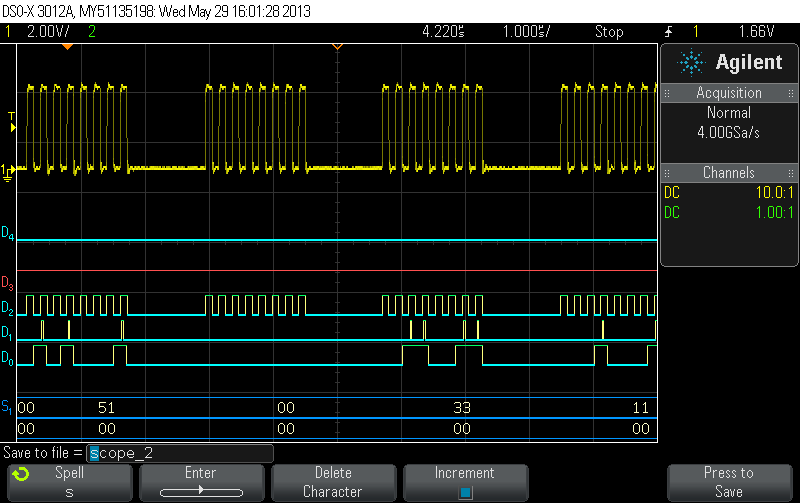
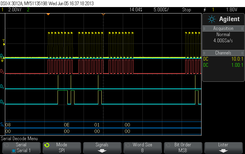
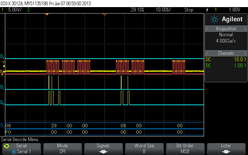
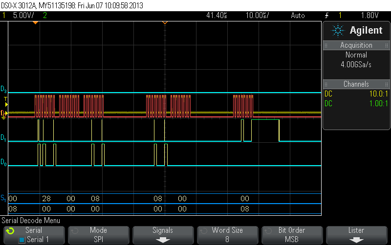
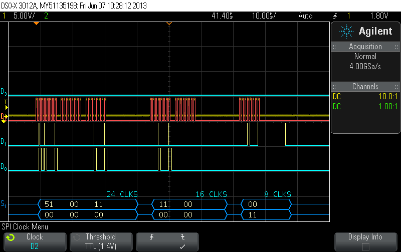
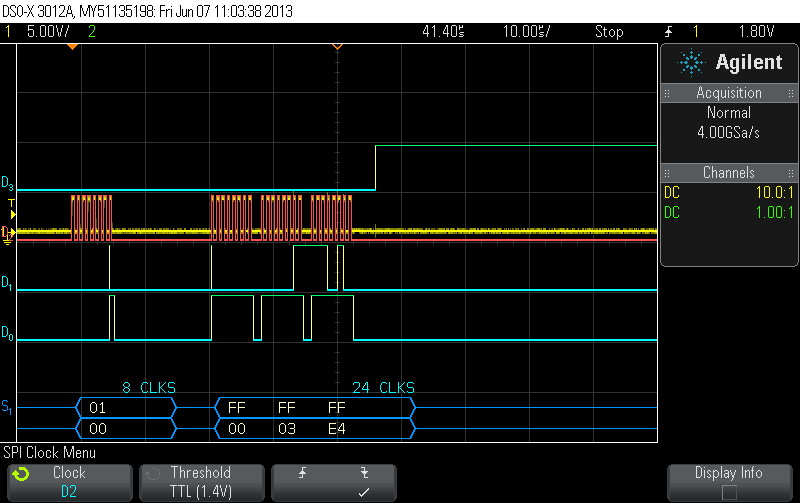
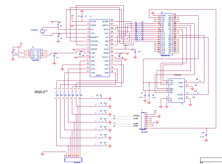
I am testing ADS1241 chip and would like to simply write to its registers and read the register back to confirm .  I am using the following code based on RREG description on page 19 of the data sheet. The data timing shows a 4nS delay time between write and read register command. I'm not getting 0 back instead of 33   from the register. I would appreciate your feedback.


Thanks,

Hamid


        int MUX0REG;         spi.write(0x51);                    // write to MUX  regiter         spi.write(0x00);                     // number of regs - 1         spi.write(0x33);                     // Ain0 (write 0 so we can read ch0 back)             spi.write(0x11);                    // read mux register back         spi.write(0x00);                     // number of regs - 1         wait(0.004);         MUX0REG = spi.write(0x00);       // number of reg - 1         pc.printf("\r\nmux0reg  = %x  \r\n", MUX0REG);

  • Hi Hamid,

    Your code appears to be ok, but it is unclear as to what is returned from the spi.write() command.  The best way to troubleshoot this is to use an oscilloscope or logic analyzer to make sure that you are reading and writing with the correct SCLK phase/polarity and timing.

    The delay time between the RREG command and the data to be transferred to the output register is 50 tosc periods minimum (t6 from Diagram 1 on page 6.)  This will depend on the clock crystal or clock input used.  If 4.9152 MHz is used, this time delay is a little over 10us.  It will scale depending on the speed of the master clock used.

    Best regards,

    Bob B

  • Hi Bob,

    Thank you for your response. The  spi.write() command is meant to do the following,

    1. Tell the SPI bus we are writing (or reading) to this specific register

    2. Define the number of bytes - 1,  we will be writing or reading.

    3. Send the  byte (or bytes) to be written, one byte at a time.

    If I am reading a register, then,  I will send zeros, and read what is sent back to a variable.   MUX0REG = spi.write(0x00);


     But again, I get all zeros.  (1)  Is this how SPI work with this chip?


  • Hi Hamid,

    Are you making sure that CS is low throughout the entire communication transaction?  Can you show me scope shots of the communication so that I can analyze?  I would like to see CS, DIN, DOUT and SCLK.

    Best regards,

    Bob B

  • HI Bob,

    Yes, CS is always low. DRDY on the other hand remains high. D0, D1, D2, D3 and D4,  are MOSI, MISO, SCK, DRDY and CS respectively.

    Regards,

    Hamid

  • Hi Hamid,

    Take another look at the ADS1241 timing diagram on page 6 of the datasheet.  For POL equal to 0, the data must be stable on the falling edge of SCLK.  You need to adjust your controller clock phase for the correct clock edge (changes on rising edge and stable on falling edge.)

    It also looks like the DOUT is either floating or noisy.  Double check and make sure you have solid connections.

    Best regards,

    Bob B

  • Hi Bob,

    The connectivity is there as far as Dout on ADS1241 to MISO pin. Could you please elaborate on the point regarding the timing diagram. Given the period of the clock (2.034e-7 s), I can find out the right range for t12  - t15 ranges from the diagram 1.  How do I apply these values to read any register and eventually the data register?


    Thank you for your response,

    Hamid


  • Hi Hamid,

    It is much easier to give the RESET command than to write the reset pattern.  But before you can issue commands you need to change the phase in which the data is sent out.  The data must remain stable on the falling edge and change state relative to the rising edge.  I believe that the ADS1241 is not responding with the correct output data because it doesn't understand what you are trying to communicate to it.

    Best regards,

    Bob B

  • Hi Bob,


    It seems like you see a problem with clock phase. I did reset the chip by pulsing the reset pin and  have tried both polarities ( 0 or 1) without getting a response. Will you please let me know how do I change the clock phase?  


    Regards,

    Hamid  


  • Hi Hamid,

    There are four operating modes combinations for the SPI communication.  The parameters are based on combinations of clock polarity and phase (CPOL and CPHA.)  Let me know what controller you are using and maybe I can help point the way to the correct settings. 

    More information regarding the SPI operating modes can be found here:

    http://en.wikipedia.org/wiki/Serial_Peripheral_Interface_Bus

    Best regards,

    Bob B

  • Hi Bob,


    Thank you for your response. I am using mode 0 transmitting 8 bit. Please see the following lines.

    Kind regards,

    Hamid


    spi.format(8,0);                 // 8bit spi mode(0,1,2,3)    

    spi.frequency(4915000);          // ads1241 clk freq 4.9152MHz


  • Hi Hamid,

    Mode 0 has the wrong phase, you need mode 1 for POL at 0.  I'm also confused by your clock frequency.  Did you mean the master clock input is 4.9152MHz?  If that is the case, the smallest period for SCLK is 4 tosc, which for 4.9152MHz will be 814ns.  This translates to a maximum frequency of 1.2288MHz for SCLK.  From your previous plot you were well within this frequency, so that is why I'm confused.

    I think the problem is you are running mode 0 and should be running mode 1 from the micro.

    Best regards,

    Bob B

  • Hi Bob,


    Thank you for your response. I changed the spi mode and freq. to 1 and 1MHz respectively. The DRDY pin(27) is always high and the chip still does not respond.


    Best regards,

    Hamid

  • Hi Hamid,

    Please send me your schematic.  For the device to properly operate you must have the required supplies, you must attach a crystal or supply a clock to pin 3, and the appropriate voltages should be applied to the digital pins. Pins 5, 6 and 7 must be logic high, and the remaining digital pins connected for the desired operation.  If you don't see DRDY (pin 27) toggling most likely one of the previous conditions are not met.

    I would also like to see a new scope shot of the communication to verify it is now correct.

    Best regards,

    Bob B

  • Hi Bob,

    Thank you for the follow up. Please see my schematic and the scope shot below. The Analog and digital input voltages are all within the ranges defined in the datasheet.


    .

  • Hi Hamid,

    Have you probed the crystal with an oscilloscope to make sure that it is oscillating and at the correct frequency?  When you checked the voltages, did you check the voltages at the ADS1241 pins or some other place?  Are you absolutely sure you are making a good connection from the ADS1241 AGND and DGND to your power supply ground?

    If you do not see DRDY toggling, then you are most likely having an issue as I detailed before.  Also, if the crystal is not oscillating, nothing on the chip will function.

    Best regards,

    Bob B

  • One thing I did not check was oscillator frequency. This is a 4.9152 MHz crystal. The period is 200nS which is about right. Also, I   should have mentioned that I measured  DVDD  and AVDD voltages at the A2D's pins.

  • Hi Hamid,

    What about your other digital pins?  Did you verify those at the pins of the ADS1241?

    Best regards,

    Bob B

  • Hi Bob,

     Yes, they are measured at the ADS1241.  Thank you for the note on the pins   PDOWN and DSYNC. They were floating before but after setting pins 5, 6 and 7  the chip comes alive. Now I have to be able to do RREG and WREG. The tosc for the 1MHz frequency I have chosen is 1uS, so the t6 = 50uS. I do put this delay between my write and read commands to see if I actually wrote what I needed to the MUX register but it does not work.  Table IV shows two bytes to be sent on SPI bus:  OP code and 2nd command byte. That's what I am doing bellow  but still can't read what I wrote to the MUX register. Is there a sample code for this chip that I can look into?

    Kind regards,

    Hamid


      spib1 = spi.write(0x51);                 //  write to MUX register    

    spib2 = spi.write(0x00);                // number of register to be written -1    

     spib3 = spi.write(0x44);                // read AIN4        

    spib4 = spi.write(0x11);                 //  read to MUX register     wait(50e-6);    

     MUXREG = spi.write(0x00);                // number of register to be written -1    

     pc.printf("\r\n spib3 = %x spib4 = %x, MUX = %x  \r\n", spib3, spib4, MUXREG);

  • Hi Hamid,

    I'm glad you are making some progress.  Did you change the crystal from 4.9152MHz to 1MHz?  Have you verified with a scope that you are getting the proper delay?  Before trying to write any registers I would try to just read them first to see if you get the default values.

    I've attached a zip file of a project done for the MSP430 using GCC.  Hopefully this can help you out.  Your best troubleshooting tool is a scope.  From the scope plots you can determine if the timing and data are correct before debugging further in software.

    8510.ADS1240_41_ExampleCode.zip

    Best regards,

    Bob B

  • Hi Bob,

    I am using the same crystal with 4.9152 MHz freq. In our earlier communications you mentioned that minimum spi clock period = 4*Tocs.   So,  I changed the spi frequency to 1MHz,  in my code only. 

    What is the relationship between to ADS1240, crystal frequency and the SPI frequency one defines in the  code?


    Best regards,

    Hamid

  • Hi Hamid,

    The fosc frequency is the oscillator frequency of the external crystal.  Tosc is equal to 1/fosc (where osc refers to the crystal oscillator.)  The maximum SPI SCLK frequency relates to 1/(4*tosc), or 1/4 of the crystal frequency which is about 1.2MHz as you have said.

    All timing in the datasheet (unless given as an exact value) relate to the tosc period which is not the same as the SCLK period. So the t6 delay is needing to be at least 50*tosc.  Your value of 50us is more than enough delay, but could be much shorter.

    Best regards,

    Bob B

  • Hi Bob,

    Thank you for your response . The timing table  shows t6 = 50Tosc = 10.17uS, while what I get on the scope is 1.5uS. Please see the screen shot bellow.

    I tried reading all registers first before writing to them. The RREG command in table 4 shows the OP CODE and 2nd command byte. The questions is what should be the 3rd byte?  I tried spi.write(0x00) as the 3rd byte, but that did not work. I also  looked into the zip file for an answer but they are using I2C there. In the past I have send NOP spi.write(0xFF) which worked for another chip, but that is not helping here either. Could you please let me know what does this chip expect as a 3rd byte to read register(s).

    Best regards,

    Hamid


  • Hi Hamid,

    If you look at the datasheet within the section towards the end you will see that the write values are don't care once the command has been issued.  A couple of things to consider.  To verify the read is working why are you trying to read from the DOR registers?  Try reading from registers that won't change values from the default settings, such as the first several registers. 

    If you are going to read data, it is much easier to issue the RDATA command which is one byte instead of two for the command.  Once the command has been issued, you must wait the 10+ us before sending any more clocks.  In your scope shot you are sending the RREG command to start reading at register 0x0D for 3 registers.  This information is two bytes.  After the two byte command you must wait the 10us before you do anything more.  Your 10us delay is after byte 3 which is incorrect.

    If using the RDATA command, this is a one byte command so you would delay after the first byte.

    Best regards,

    Bob B

  • Good morning Bob,

    Thank you for clarification on the RREG,  3rd byte. That was very helpful.  I was trying to read the first 8 registers (as you pointed out),  and then eventually read data registers once I could write to the MUX. Adjusting the timing writing to register issue got resolved.

     I am still trying to read data registers though.  The program  waits for DRDY pin(27) to go low  and then, send RDATA command wait 10.uS and read the 3 bytes back. The numbers however do not make sense.

    if (DRDY0 == 0)    

    {         spi.write(RDATA);        

               wait(10.17e-6);                    // t6 = 50 Tosc = 50/4.9152e6 = 10.17uS               

               _DOR2 = spi.write(0x10);                 // Data registers           

               _DOR1 = spi.write(0x10);                       

               _DOR0 = spi.write(0x10);                

    }


    Kind regards,

  • Hi Hamid,

    Do you have a scope picture of the read data?  What do you expect and what are you getting back as results?  Is your reassembled data matching the scope data? 

    You may also want to increase your delay slightly to make sure you are within the operating tolerances of both your microcontroller timing and the crystal for the ADS1241.

    Best regards,

    Bob B

  • Hi Bob,

    Please see the following scope shot.    DOR23-DOR0 should contain a count proportional to the input voltage connected to  the given channel. The formula we once discussed is        V = Count * Vref / (2^23-1).  

    The most significant byte is always 0 regardless of the input voltage, so that's one indication of not reading correctly. The count we see on all channels when the pin is floating or if there is a voltage there (0.5 - 1.5) remains close to 1000, and  the calculated V is always zero. This is of course when   gain = 1. I changed the delay between RDATA command and reading the 3 bytes to 12 uS without seeing any change in the result.


    The scope data is a bit curious. The numbers I see on the scope serial bus is always half of what we actually transmit on the SPI bus. .

    Kind regards,

    Hamid


  • Hi Hamid,

    I'm not quite sure what you are trying to show me with the scope shot.  You are writing 0 to the MUX register and reading back 0.  I'm more interested to see if you can read back the default values of the registers (or at least write something non-zero and read back.)

    Best regards,

    Bob B

  • Hi Bob,


    I was reading the data register in the pervious shot. Please see the following image.  We are  writing 11 to MUX register here,  and read it back. Again, the numbers shown on the serial bus are half of what I actually send.  0x51 is shown as 28 and so on.

    Best regards,

    Hamid


  • Hi Hamid,

    You are writing and reading correctly to the ADS1241.  Your serial protocol analyzer is reading the data on the wrong clock edge (incorrect phase.)

    Best regards,

    Bob B

  • Hi Bob,

    Thank you for your feedback. I have corrected the phase in the new image bellow.  The data sheet states that when new data is loaded to the data register DRDY goes low so, I try to read data at that point. The counts I get however are off. I have a 0.7 Volt input hooked up to channel 1. We have written 11, to MUX register, so I should be getting meaningful count if the timing is correct. Do see any timing  issues with the second image?  D3 is connected to DRDY pin and as you see the most significant bit is 0.

    Best regards,

    Hamid  


  • Hi Hamid,

    The timing looks correct.  Do you have a schematic that I can look at?  What value of reference voltage are you using?

    You are getting 996 codes for what ever value reference you are using.  According to the MUX register setting you are shorting the inputs, so you would expect to see 0 code (+ noise and offset.)  If you have not issued a SELFOCAL, then I've seen shorted inputs as high as 2000 codes of offset, so for shorted inputs you are in the correct range.

    As the ADS1241 measures one input relative to another (differential measurement) you need to select your MUX appropriately.  AINP (positive) and AINN (negative) cannot be connected to the same channel for a measurement (otherwise you have shorted inputs which is 0.) 

    Let's say you want to make a single ended measurement for AIN1 and you connect the 0.7V to this input.  If you connect ground (or common for the voltage applied) to AINCOM and write 0x18 to the MUX register you should see the correct voltage output code.  0x18 selects AIN1 as the positive input and AINCOM as the negative input.  You will receive a measurement relative to the difference of the two inputs.  In this case you will get a positive result as AIN1 is more positive than AINCOM.  If you switch the MUX so that you write 0x81, then you will see a negative value returned as the positive input is less than the negative input.

    Best regards,

    Bob B 

  • Hi Bob,

    Please see the schematic bellow.   I  issue  SELFOCAL at the top of my code, and use a 2.048 V as our reference voltage. Thank you for the point on differential vs. single ended measurement.   We are reading voltage with respect to AINCOM, so now our number looks more reasonable. It seems to me making differential measurement leads to a more solid reading with less drift. I am not sure why but I do get more drift when I read voltages with respect to AINCOM. Do you have any preference between the two? And gain my schematic follows, please feel free to make comments on the circuit.  

    Bes regards,

    Hamid


  • Hi Hamid,

    Now that we have the digital portion working we can concentrate on the analog portion.  One thing to keep in mind is the measurement is always a differential measurement no matter if it is connected as a differential input signal or a single ended signal.  What makes the two measurements differ is with respect to range.  With a differential input voltage you can have a + or - measurement swing, whereas the single ended input voltage can only have a + result.  The method used for setting up the MUX for the measurement are the same for both where the AINPOS and the AINNEG must be connected to something.  According to your schematic, you can make a measurement when AINPOS is connected to AIN0, AIN2, AIN3, AIN4, AIN5, AIN6 or AIN7.  AINNEG can be connected to either AIN1 or AINCOM.

    You must make certain that the value used for your calculation matches the actual reference value used.  You stated you used 2.048V but the schematic shows a REF5025 which is a 2.5V reference.

    I'm not sure how low of an impedance your source voltage is, or how stable the voltage is relative to 100 ohm resistor.  The 100 ohm resistor can self heat and change value and can also have drift and be noisy.  You might see more stability if you add a cap from the input (at the pin) to ground of about 10nF.

    Depending on the AVDD supply value, you may see issues if you are using the ADS1241 with the buffer enabled.  You have a restricted input range with the buffer enabled.  It will be better to have the buffer disabled when making single ended measurements.

    Board layout is also critical for getting low noise and stable measurements.  See the following information about board layout:

    http://e2e.ti.com/support/data_converters/precision_data_converters/w/design_notes/1302.general-pcb-layout-questions.aspx

    Best regards,

    Bob B

  • Hi Bob,

    The reference voltages I chose initially was based on what I have initially available, and now I am using a REF5050 to get a 0.1-5V range. I am using the same 5 VDC as a source for AVDD and DVDD so that I use only one power supply. This is reflected in the schematic.  I can see that the max input voltage becomes  AVDD - 1.5 V when buffer is enabled, so we stay within that range or disable buffer. 

    Thank you for the link on PCB. I am trying to refine the circuit and get the most stable reading at this point but don't know where to stop. The input voltage to A2D chip does fluctuate when I look at it closely with my analog probe, so the reading should change slightly. I am taking the 2.5 volt output of REF2025 and feed that to ADS1241. It turns out the readings fluctuate by 10mV, but then again the voltage coming out of REF2025 shows  some fluctuation on the scope.


    Best regards,

    Hamid

  • Hi Hamid,

    If you short your inputs and then take a series of successive measurements and plot them you will see the amount of noise in the conversion.  If you do not get the kind of results shown in the Typical Characteristics Noise Histogram graph shown at the top of page 9, then you have some more work to do cleaning up the noise issue.

    If you are able to achieve these results, then you should have a more desirable response.

    Best regards,

    Bob B


  • Thank you Bob!

    Best regards,

    Hamid

  • Good morning Bob,

    I have shorted pin 11 though 18 and am looking at the conversions. Could you please elaborate a bit on the histogram's  horizontal axis. What is FS? and also do I need to connect the shorted pins to com to get Vin = 0v?


    best regards,

    Hamid


  • Hi Hamid,

    There are a number of ways you can short inputs.  You can make external physical connections, or assign the mux to the same AIN channel for both + and - input channels.  In either case you need to assign the mux channels to the desired inputs.

    The histogram plot is usually codes, which can be converted to volts if you want for the X scale.  In the case for the datasheet figure the plot is in parts per million for a full-scale reading.  Each code bin is 0.5ppm of FS in width.  The values collected would be added to each code bin and then graphed appropriately.

    If you have not worked with histograms then it may be easier to deal with the effective resolution or noise graphs shown on page 7.

    Best regards,

    Bob B

  • Hi Bob,


    Thank you for your response. So, we are reading all these counts which can be converted to a voltage.    Is the ppm of fs  the ratio of each data point (Votage read or the count ) and Vfull scale (5 Volt)? 

    Best regards,

    Hamid

  • Hi Hamid,

    The graph discussed is normalized, so it all depends on your operating conditions with respect to reference and gain selected.  I think it will be easier to think in codes and distribute that way.  Once you have determine one sigma, you will have the RMS value and then take that number and convert to voltage or you can determine the total number of bits for the noise of one sigma and subtract that from 24 to find the effective resolution. 

    For the latter case, let's say the one sigma of distribution is 48 codes.  The number of noise bits is ln(48)/ln(2) or about 5.58 bits.  You subtract this from 24 to get the effective resolution.

    When using voltages, the effective resolution is equal to ln(full-scale range/RMSnoise)/ln(2), and you should get the same number of bits in either calculation.

    Best regards,

    Bob B

  • Thank you Bob!

    Have a good weekend,

    Hamid

  • Hi Bob,

    I have individual channels working at a descent resolution now. Now we  need to utilize all channels together.  As we discussed in the past,  writing   to the mux register and reading  the content back we switch channels. Once the DRDY goes low, we read the 24 bit data register which converts to the voltage for the given channel.  I am forced to wait 50 mS after each conversion to avoid voltage readings that are shifted or incorrect. The t17 in  timing diagram, however  is about  1.02 mS, so it seems like there is a faster way of doing this. Is there a standard method for multiplexing? What is the optimum timing to read all 4 differential channels?


    Best regards,

    Hamid  

  • Hi Hamid,

    To maximize your throughput you need to make sure your mux change happens within the t17 period.  That doesn't give you much time, and in fact doesn't work well if you are polling the DRDY status.  You should be using DRDY as an interrupt to your processor and the ADS1241 operating in RDATAC mode where the data is automatically placed to the output register. You can read the data and write the register at the same time with RDATAC mode as the SPI bus is full-duplex.

    It is also possible to not use RDATAC mode, but you will have to write the register first for the mux change and then read the data results.  You still need to make sure the mux change happens in the t17 period, and the only way I know that you can safely do that is with an interrupt driven system.

    Best regards,

    Bob B

  • Hi Bob,

    Thank you for your response. If I issue RDATAC command for some reason I can't write to mux register any more. After doing RDATAC, the mux register shows the default value continuously when I echo the content back. When doing RDATA though, we can switch channels as you know but it takes 1.5 seconds to read all channels.

    Best regards,

    Hamid

  • Hi Hamid,

    You must be doing something wrong.  For the worst case you would write the register (3 bytes), read the register back (3 bytes) and read the data results (4 bytes) this is a total of 10 bytes and 8 clocks per byte.  If your SCLK is 1MHz, then 80 clocks must be issued for the complete cycle. With the added delays between command and read that still leaves you less than 200us which is well below a 15sps data rate (period of 67ms).

    If you have a long loop of events to process, this is most likely your issue as it is delaying the ability to read the data within the specified data rate.

    Best regards,

    Bob B

  • Hi Bob,

    I have removed everything from the while loop except for a read register command to read the default value in the setup register. I can consistently read 20 from setup register when there is no RDATAC command issued before the loop. When we issue RDATAC command before entering the loop, though, things fall apart. I wonder if this is a question of timing. As you can see from the lines bellow, the last of the 3 bytes sent  is delayed by 12uS ~ which is larger than 10.17uS or 50tosc.  

    Best regards,

    Hamid  


     spi.write(RDATAC);    

    wait(12e-6);                    // delay by t6 = 50tosc = 50/4.9152 = 10.17us    

     while(true)    

     {          

                spi.write(0x10);                // read back SETUP        

                spi.write(0x00);         wait(12e-6);        

                 int SETUPREG = spi.write(0x00);        

                 pc.printf("\r\n  setup = %x \r\n", SETUPREG);

    }

  • Hi Hamid,

    I think you are missing the point on the usage of RDATAC.  RDATAC automatically posts the results to the output register.  As soon as the ADS1241 sees SCLKs it will start to send out the conversion results.  When using RDATAC, you send 3 NOPs to read the results, then you can read the data from other registers if you like.

    I think it may be easiest for you to not use RDATAC, but rather:

    1. Write the MUX change
    2. Read the MUX as verification (if necessary)
    3. Read the data

    I think that might be easier to follow.

    Best regards,

    Bob B

  • Hi Bob,


    I have been tying to get the timing right on this chip all day.Trying the 3 steps you wrote, how much time does it take to read one  channel? Polling DRDY pin, I have a hard time to get the  correct conversion values all the time. I did

    write to MUX, wait(50*tosc), and read data (if DRDY==0), repeat . Is this what you were suggesting?


    best regards,

    Hamid


  • Hi Hamid,

    Engineering is fun, right? It is stressful trying to get things to work the way we want, but then it is a great feeling of accomplishment when it is finished.

    Here is the total process:

    1. Poll DRDY (better to use a controller interrupt, but we can work with polling) and wait until it goes low
    2. Write the register to change the MUX to the next input
    3. Wait 4 tosc periods
    4. Send RDATA command
    5. Wait 50 tosc periods for results to be placed in the output register
    6. Read three bytes of the result data
    7. Loop back to item 1

    What needs to happen as soon as possible at the end of the conversion cycle is the MUX change so that the next conversion is accurate.

    I hope that explains the process a little better.

    Best regards,

    Bob B

  • Hi Bob,

    The unpredictability does make engineering fun.   Thank you for elaborating on your response.  The conversion time is much faster with these 7 steps. I think I need to have a tighter control on this process. There are readings every second or so,  that are not very accurate and differ with actual value  by 400mV or more.  What would be the best way of dealing with inaccuracy here?  


    Best regards,

    Hamid