This thread has been locked.

If you have a related question, please click the "Ask a related question" button in the top right corner. The newly created question will be automatically linked to this question.

ADS1298 - Functional Block Diagram - Issue

Other Parts Discussed in Thread: ADS1298

Hi,

I have a problem with the function block diagram of the ADS1298.
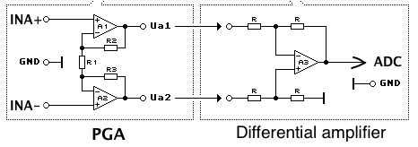
The signals INxP INxN run through the EMI filter into the MUX. And then to the PGAs. Where the difference is build and passed to the ADC.
My problem is the block diagram shows that two signals are going from the PGA to the ADC. That I do not understand. The ADC has only one input. Which of the signals  is passed to the ADC? Only the difference (lead)?

Is there no Instrumentation Amplifier used to prepare the Signals for the ADC?

I would like to understand how the ADS1298 works exactly.
I hope someone can explain this to me. Thanks in advance.

  • Mr Regner -

    Are you referring to Figure 23 in the datasheet?

    The signal path through the EMI filer, PGA, and into the ADC is a differential signal path.  There is a single signal being converted by the ADC; the signal is the difference between IN+ and IN-.

  • Mr. Hupp

    thanks for the reply.
    Yes, I am referring to Figure 23
    Now I understand that there is a differential signal path to the ADC.

    Before the ADC is there a differential amplifier which forms the differential signal between IN+ and IN- and give it to the ADC? As seen in the image?

    Thanks in advance.