This thread has been locked.

If you have a related question, please click the "Ask a related question" button in the top right corner. The newly created question will be automatically linked to this question.

ADS1247 conversion issues

Other Parts Discussed in Thread: ADS1247

Hi 

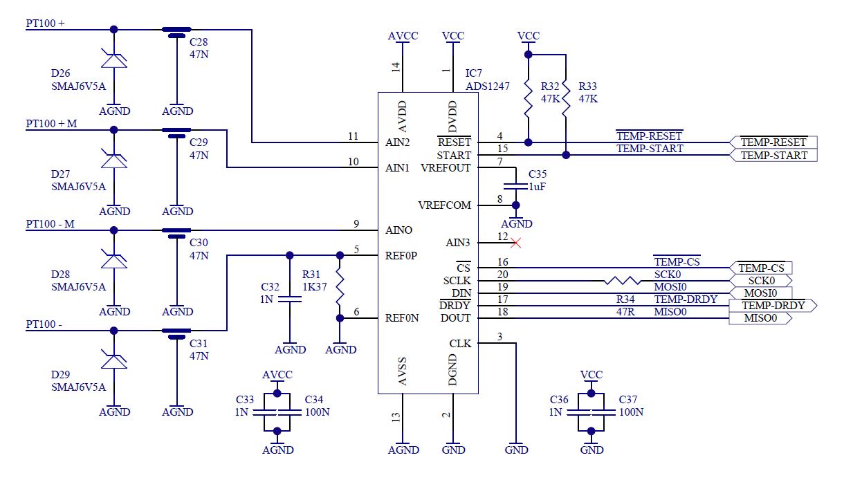
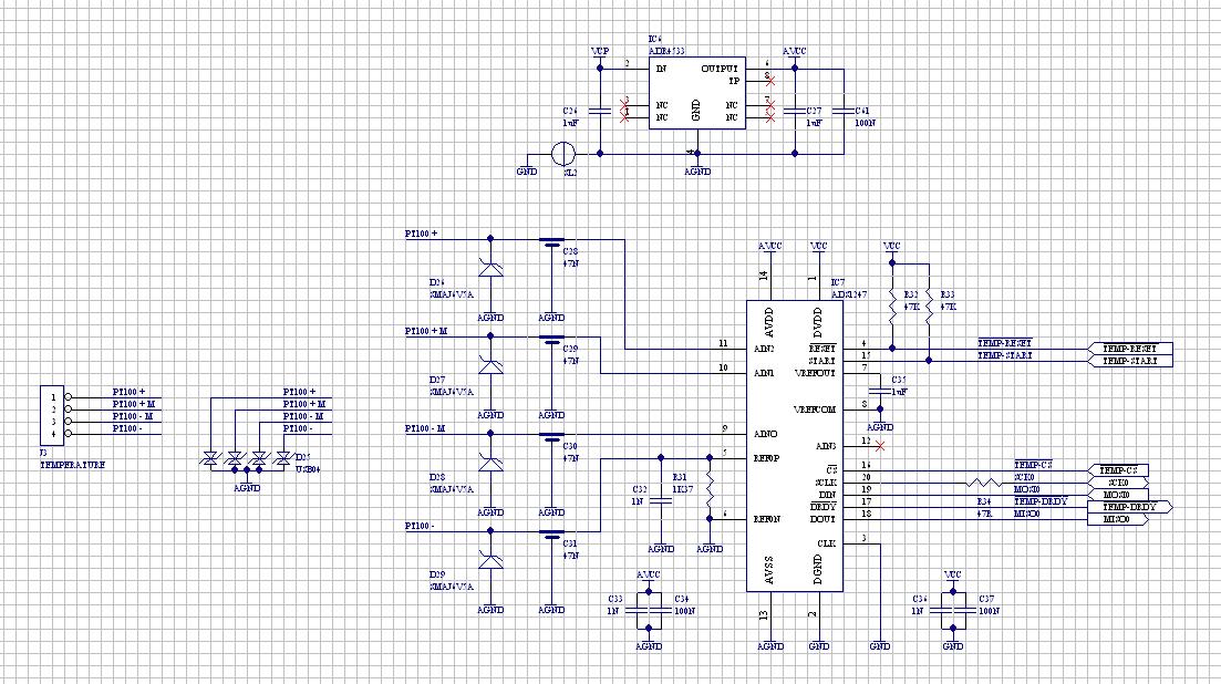
I am using the ADS1247 for a 4 wire PT100 temperature interface, the issue I am having is that no two readings from the ADC are ever close

They differ with thousands and even tens of thousands of steps each time

Here is my general operation:

Initialisation

ADS1247_Reg[0] = 0x08; //[00][00 1][000] Burnout current source off, Positive input channel AIN1, Negative input channel AIN0, No bias
ADS1247_Reg[1] = 0x00; //[xxxx][0000] Bias voltage register: No bias voltages
ADS1247_Reg[2] = 0x30; //[0][01][1 0][000] Internal oscillator ON, Internal reference ON, Onboard ref selected, Normal operation
ADS1247_Reg[3] = 0x38; //[0][011] [1000] Always 0, Gain of the PGA, Output data rate (SPS)

ADS1247_Reg[10] = 0x06; //[0000] [0][110] Dout only, current = 1mA
ADS1247_Reg[11] = 0x2C; //[0010] [1100] Output pin for 1st DAC: AIN2, output pin for 2nd DAC

General Operation:

Set START pin to high

Set START pin to Low

Wait for READY to go low

Send_SPI_Char(0x13)

Data[0] = Send_SPI_Char(0xFF)

Data[1] = Send_SPI_Char(0xFF)

Data[2] = Send_SPI_Char(0xFF)

Do I need to send the 0x13 when reading the data? The ADS1247 still gives me data even if I do not issue the command

Regards

RIchard

  • Hi Richard,

    Welcome to the forum!  It would be helpful to see a schematic of how you have things connected.  A couple of reasons you may have inconsistent readings could be caused by not having at least a 1uF cap from VREFOUT to VREFCOM (and VREFCOM should also connect to AVSS).  Another possiblity is with respect to how you may have your RTD connected.  You must make sure that the input is within the common mode input range of the ADC.  In short, if using a single supply for AVDD/AVSS, you cannot connect the sensor directly to ground.

    The best method for measuring is by using a ratiometric method where you use a precision resistor to bias the RTD into the correct common mode input range and also use the voltage developed across the bias resistor as an external reference.  In essence this simplifies the transfer function to a ratio of the RTD to the bias resistor.  It will cancel noise and drift effects related to the IDAC.

    Best regards,

    Bob B

  • Hi Bob

    Thanks for the Prompt response

    I attached the PDF of my schematic which should hopefully help

    Also, my AVCC and VCC are 3.3VDC but my CPU is running at 3.0VDC

    Regards

    Richard

  • Hi Richard,

    The schematic didn't get attached for some reason.  Can you try again?

    Thanks,

    Bob B

  • Hi Bob

    I managed to figure out the issue, I was not holding my START pin high for long enough at startup

    The settings looked right but were clearly not

    Many thanks

    Richard

  • Hi Bob

    I have done some further work on the ADS1247 circuit I mentioned earlier and have some questions...

    I have an application where I need to measure temperature to a very high accuracy over a wide ambient temperature range (-25°C to 65°C). Because of long cable length we decided to go the 4 wire pt100 route, because of the negligible effect the cable resistance have on the voltage on the

    measuring wires (2 and 3). I have started development on the ADS1247 development board with the MMB3 dev kit and have obtained good enough preliminary results to go onto the prototype phase.


    Please find attached diagram for reference


    The ADS1247’s AVDD is 3.3V supplied from a precision voltage source, and the DVDD is 3.3V. Resistor R31 (1k37) is a high precision resistor 0.1% with a thermal coefficient of 15ppm. The internal voltage reference was used for the ADC (2.048).

    The temperature range we want to measure on the pt100 is between -40°C and 100°C which will give us an input voltage to the ADS1247 of 126.405mV and 207.765mV. The PGA gain is set to 8 which will give a max output of 1662.12mV to the ADC which will be referenced to 2048mV.

    The ADC should then give a reading of 13569706. These above mentioned results were all calculated theoretically, to prove the understanding and operation of the ADS1247.


    We then proceeded to build two proto-type pcb’s to confirm the above described results.

    The first problem we encountered was the difference between the two pcb’s temperature which we can calibrate out which is not preffered, we decided that that could be because of the IDAC initial error of 6% which will theoretically have a 0.12°C effect between the two different

    IC’s (see attached spreadsheet).


    With the one proto-type, from now on refered to as B1 placed in our temperature chamber set to -25°C for 24 hours, we saw a temperature drift of 0.34°C form the reference temperature measured at room temperature (22°C). We then adjusted the chamber temperature to 60°C and

    obtained another temperature drift of another 0.4°C which makes the total temperature drift 0.74°C.


    We then refered back to the spreadsheet and confirmed that we could expect a temperature drift of 0.56°C because of the temperature coefficient of the internal voltage reference (15ppm / °C).


    We are in the process of changing the voltage reference now from internal to external using the ratiometric approach with a 1.5mA constant current developing a 2.055V voltage reference across our R31. This voltage generated across R31 used for the external voltage reference

    to the ADC is below the 1V mentioned in the datasheet.


    Would this be a recommended solution to our drifting results issue??

    3225.ADS1247 Performance Analysis - 2.xls

    Regards

    Richard

  • Hi Richard,

    The ratiometric approach is the best.  The basic reason is that you take the current source and related drift out of the equation.  You can do this because the voltage developed across the RTD and the voltage developed across the reference resistor has the same excitation current.  The transfer function of the RTD relative to the reference reduces from a voltage ratio to a ratio of the resistances.  When using the internal reference your result will include any noise/drift of the reference as well as the noise/drift of the excitation source.

    As a matter of the final result it is difficult to just swap in and out RTDs and not calibrate.  The reasons are the differences of the accuracy of the RTDs themselves, and the component tolerances of the devices used on the PCB.  If the total possible error is within a range that is acceptable to you then you should be ok, but usually this is not the case.

    I see from your schematic that you have a number of components for input protection on the analog inputs that are likely to have leakage currents that will change with temperature.  Diodes can be very leaky.  This will affect the measurement result.

    I also see you have no RC filtering at the analog inputs.  You may want to consider adding some filtering, if for no other reason, to filter any high frequencies that may alias back into the pass band.

    Best regards,

    Bob B