This thread has been locked.

If you have a related question, please click the "Ask a related question" button in the top right corner. The newly created question will be automatically linked to this question.

ADS8361 data syncronisation problem in Mode II

Other Parts Discussed in Thread: ADS8361

Hi All,

I am new to DSP & this forum. I am trying to interface ADS8361 EVM Rev.B with TMS320VC5510 DSK using 5-6K Rev.B board.

Mode II: M1 open, M0 closed, A0 Closed.

MCBSP_Config mcbspCfg0 = {
    0x0000,        /*  Serial Port Control Register 1   */
    0x0200,        /*  Serial Port Control Register 2   */
    0x0060,        /*  Receive Control Register 1   */
    0x0004,        /*  Receive Control Register 2   */
    0x0000,        /*  Transmit Control Register 1   */
    0x0001,        /*  Transmit Control Register 2   */
    0x0013,        /*  Sample Rate Generator Register 1   */
    0x2013,        /*  Sample Rate Generator Register 2   */
    0x0000,        /*  Multichannel Control Register 1   */
    0x0000,        /*  Multichannel Control Register 2   */
    0x0600,        /*  Pin Control Register   */
};

void McBSP0Rcv_ISR(void)
{
 /* Wait until a value is received then read it */
 while (!MCBSP_rrdy(hMcbsp0));          
 ad_temp = MCBSP_read32(hMcbsp0);//>>1;
 ad_buffer[i++]=ad_temp>>1;
 if ( i % 2 == 0 )
     Chan1[j++]=ad_temp>>1;
   else
     Chan2[k++]=ad_temp>>1; 

if (i >= BLOCK_SZ )       /* Reset index?   */
 {
  i=0;
  j=0;
  k=0;
  MCBSP_read(hMcbsp0);    /* Flush receive register */  
  MCBSP_read(hMcbsp0);    /* Flush receive register */
  MCBSP_read(hMcbsp0);    /* Flush receive register */ 

 }
}

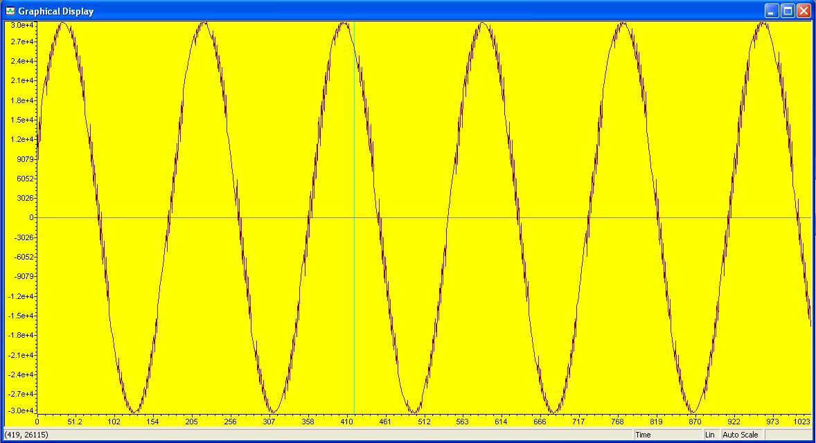
I can see some data but they looks like mixed from both channel. I have tried to seperate them but unable to get any success. It would be a great help if anyone have any example code. I am not sure about the McBSP settings and CS pin.

Thanks in advance.

Shekhar

  • Hi Shekhar,

    Please find attached an example project for the ADS8361 connected to an TLS320VC5510 DSK. This project was created with CCS3v3.

    Regarding your McBSP settings:
    The best is to use the McBSP in FSG mode. This means the sample rate generator (SRGR) is used to trigger a transfer. This is very useful here since all the data converter signals such as CLOCK, CS#, RD, CONVST are provided by the DSP and are related to each other. If you tie CONVST and RD together you have a constant sample frequency provided by the McBSP.
    Another beauty is that you need to configure the McBSP receiver portion only. CLR and FSR can be configured as output. This gives you the possibility to use the transmitter to drive another peripheral.
    Talking about the data converters CS# signal. This signal is tied to a GPIO of the 'VC5510 DSK. You can change this by writing to the CPLD register of the DSK. Please refer to the TMS320VC5510 Technical reference to learn more about it. However, this signal can be low permanently. Since the default is also low you don't need to worry about this right now.

    The example project gets data from the device, shifts the data word right by 2 and masks it with 0xFFFF. This way you get your pure signal without any information.
    As a first test you can display the data in CCS with the graph window. Since the data are interleaved they are combined in the view at the first place. However, you can set the index increment parameter of the graph to 2. By doing that every other sample gets displayed in the graph - which is always the same channel then. This means you can check both channels independently without writing a single line of code.

    If you have more questions please let me know.

    Best regards,
    Lars Lotzenburger

    ADS8361-DSK5510-CCS.ZIP
  • Dear Lars,

    Thank you very much for your very quick and usefull answer. I have run the code you gave. it works fine as I wanted [:D].

    When I put breakpoint after block transfer (dc_rblock(pADS, BufferRaw, BUFF_SZ, 0);) then the data was seperated properly for the different channels on different graph windows.

    But when I put the breakpiont after dc_read ((dc_read(pADS) >> 2) & 0xFFFF); then the data was not seperated properly. I have read the notes in file t8361_ob.c that says block transfers (dc_rblock()) are syncronized! and block transfers (dc_rblock()) are syncronized! at all!

    This was my problem. I could not seperate the data from different channel in different buffers. I would like to know how do I have to syncronize the data so that I could seperate them in different buffers? Thank you very much for your time.

    Kind regards,

    Shekhar

  • Shekhar,

    the software does not separate the channels, but is synchronized for dc_rblock() - where you read multiple data from the converter. This means that the channels have a fixed position in the data field. You can spearate them easily by introducing two new buffers and read the data from the buffer filled by the software. Every even-indexed buffer element goes in one buffer, every odd-indexed buffer element in the other.

    For your information: There will be a new interface software version for this data converter available in 1Q10. This software will use also the DMA on the 'VC5510 to free up the CPU. I also plan to let the DMA separate the channels in the buffer. I don't know your schedule, but if you could wait I think it's worth to use the newer version then...

    Just let me know.

    Best regards,
    Lars

  • Shekar,

    One additional item to consider - please refer to Figure 11 in the datasheet - the ADS8361 starts off from power up in mode 1.  The output data from the first transfer could be from an either CHA or CHB.  The state of the mode pins is determined after the first conversion is complete, so starting with the second cycle, you should have data from CHA, CHB, CHA, ChB...  You could simply throw away the first sample and begin storage into your buffers with cycle two, or use the channel ID bits as a mask to assure proper storage.

  • Dear Tom Hendrick,

    Thank you very much for your very useful reply. I have followed your example program for TMS470 that used channel ID bit and the program works perfectly with the polling version in Mode I and Mode II. But I am still struggling with the interrupt driver program. The interrupt program works well in mode I. But Signal is distorted in interrupt version in Mode II. Here is the interrupt service routine and channel sorting code. Could you please suggest if anything I am doing wrong? Thanks for your time.

    Kind regards

    Shekhar

    void McBSP0Rcv_ISR(void) {
       while (!MCBSP_rrdy(hMcbsp0));          
      ad_temp = MCBSP_read32(hMcbsp0)>>1;
      sort(ad_temp);
    }

    void sort(long data)
    {
      long CH = (data & 0x00010000);
      switch (CH)
      {
      case 0x00000000:
        Chan1[indx] = (int)(data & 0xFFFF);
        count+=1;
        break;
      case 0x00010000:
        Chan2[indx] = (int)(data & 0xFFFF);
        count+=1;
        break;
      }
      if (count == 2)
      {
        indx+=1;
        if (indx==BLOCK_SZ){
        indx = 0;
     MCBSP_read(hMcbsp0);    /* Flush receive register */
     MCBSP_read(hMcbsp0);    /* Flush receive register */
     MCBSP_read(hMcbsp0);    /* Flush receive register */
     }
        count = 0;
      }
    }


  • Hi Shekar,

    When you say the signal is distorted, do you mean you are getting mixed CH0/CH1 data or that it is just corrupted/garbage data?  Are you still using the McBSP settings noted in the original post?  If so, you are receiving a 20-bit word.  The data from the ADS8361 is 16-bits plus the channel and pair ID bits (18-bits in all).  It looks like you are shifting only one bit above in your loop.  I believe that should be 2-bits to properly align the LSB and then use the 0x10000 mask you have set.

  • Dear Tom Hendrick,

    Thank you very much for your quick reply. My McBSP setting were similar to your example from slaa162 and 1 bit shifting was giving the data right (I think because FWID set to 1). The signal I am receiving is corrupted most of the time in a regular interval. Some times more and sometimes less noise like signal. I can see the sine wave some times clear and sometimes with noisy. I have changed the McBSP settings (FWID set to 19) and shifted 2 bit right but still same type of signal distortion happening. I am including a picture of the signal if that helps.

    Kind regards,

    Shekhar

  • Hi Shekhar,

    With the TMS470 code, the interface was running with an SPI or 'stop clock' type of serial clock. and if I remember correctly, there is an extra clock cycle involved with that setup.  For the McBSP port on the C5510 the way you have things configured, the rising edge of the FS input is what starts the conversion/RD cycle. 

    The first falling clock under FS high qualifies the 'read'.  The second and third clocks will contain the channel ID bits and the forth clock has the MSB data.  In your code that you sent me, you are receiving the data, shifting by two, and comparing it to 0x00010000 to do your channel mask.  You don't need that shift - simply change your mask to 0x00020000.

    Next is the data shift on storing to your Channel arrays.  Currently you shift right by two, the shift should only be right by one.  Something like this should work:

    void sort(long data)
    {
      long CH = ((data) & 0x00020000);
      switch (CH)
      {
      case 0x00000000:
        Chan1[indx] = (int)((data>>1) & 0xFFFF);
        count+=1;
        break;
      case 0x00020000:
        Chan2[indx] = (int)((data>>1) & 0xFFFF);
        count+=1;
        break;
      }

    ...


    If you still have trouble using that minor set of changes, please shoot me an e-mail and we'll talk more about this off line.