This thread has been locked.

If you have a related question, please click the "Ask a related question" button in the top right corner. The newly created question will be automatically linked to this question.

ADS131E06 initialisation problem

Other Parts Discussed in Thread: ADS131E06

Hi,

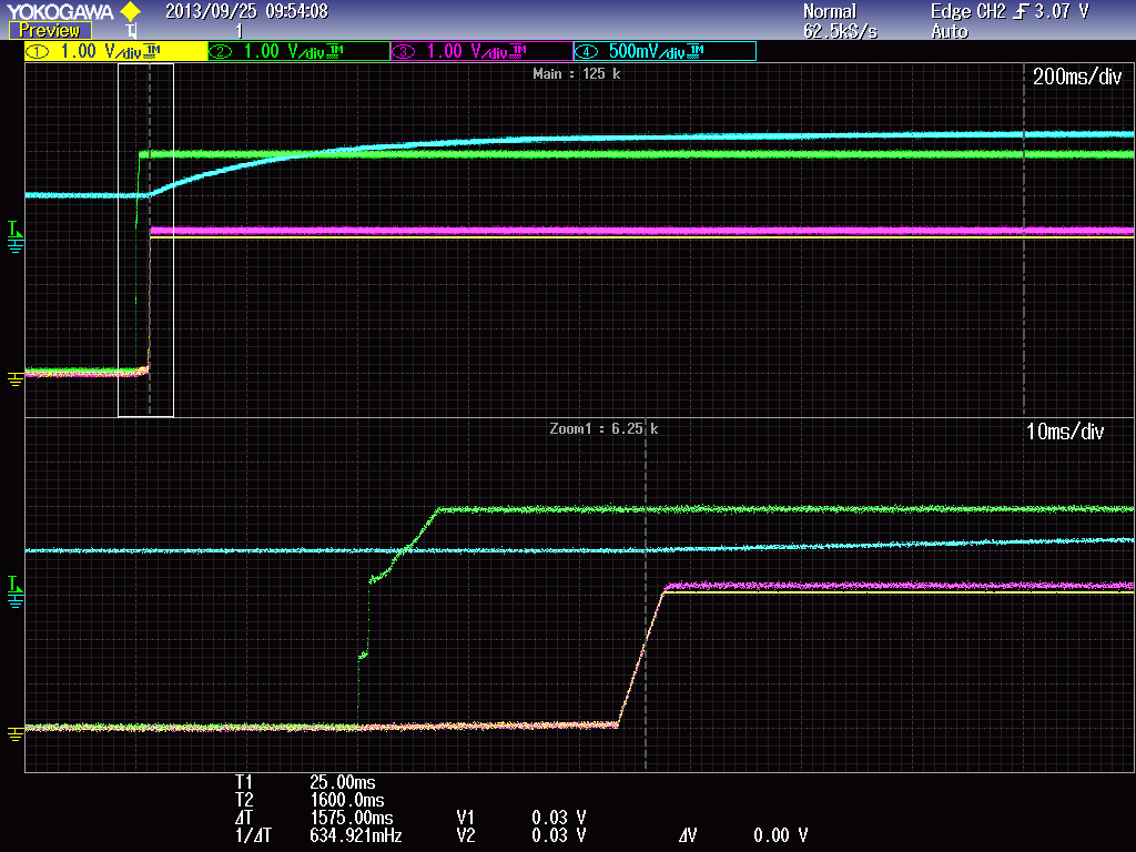
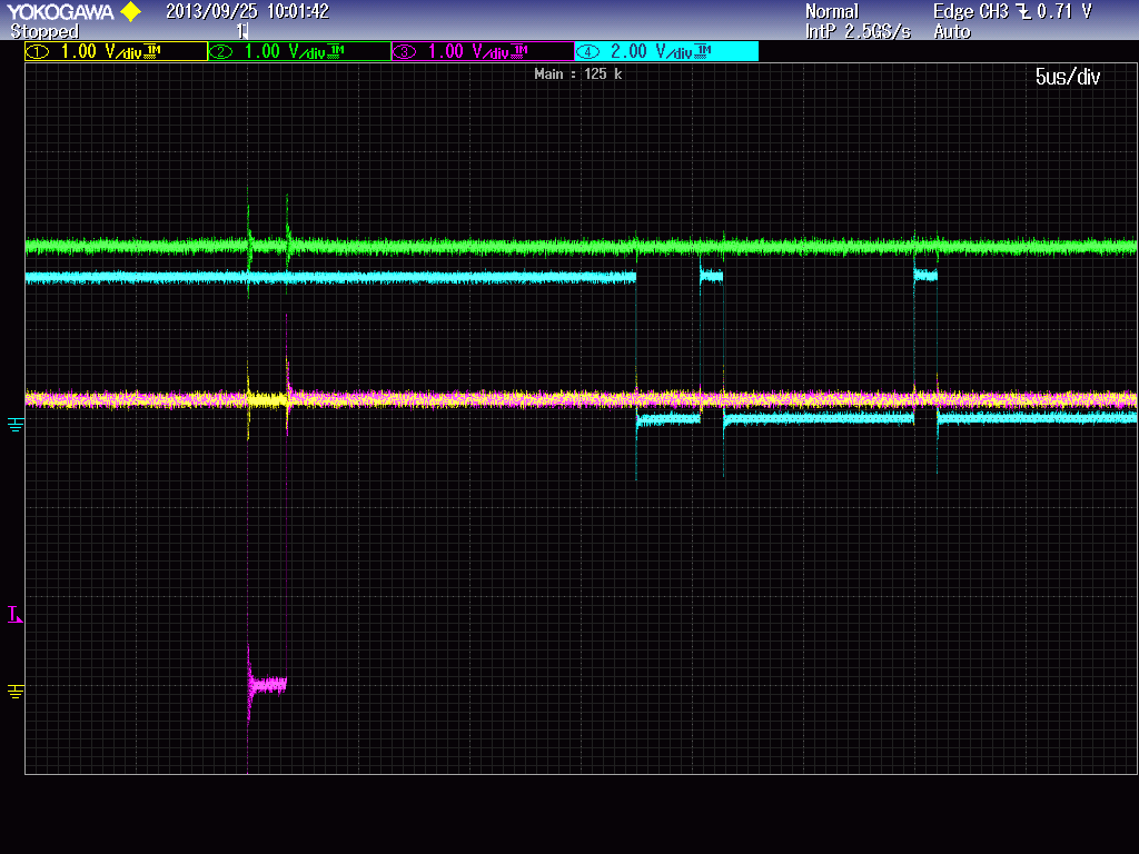
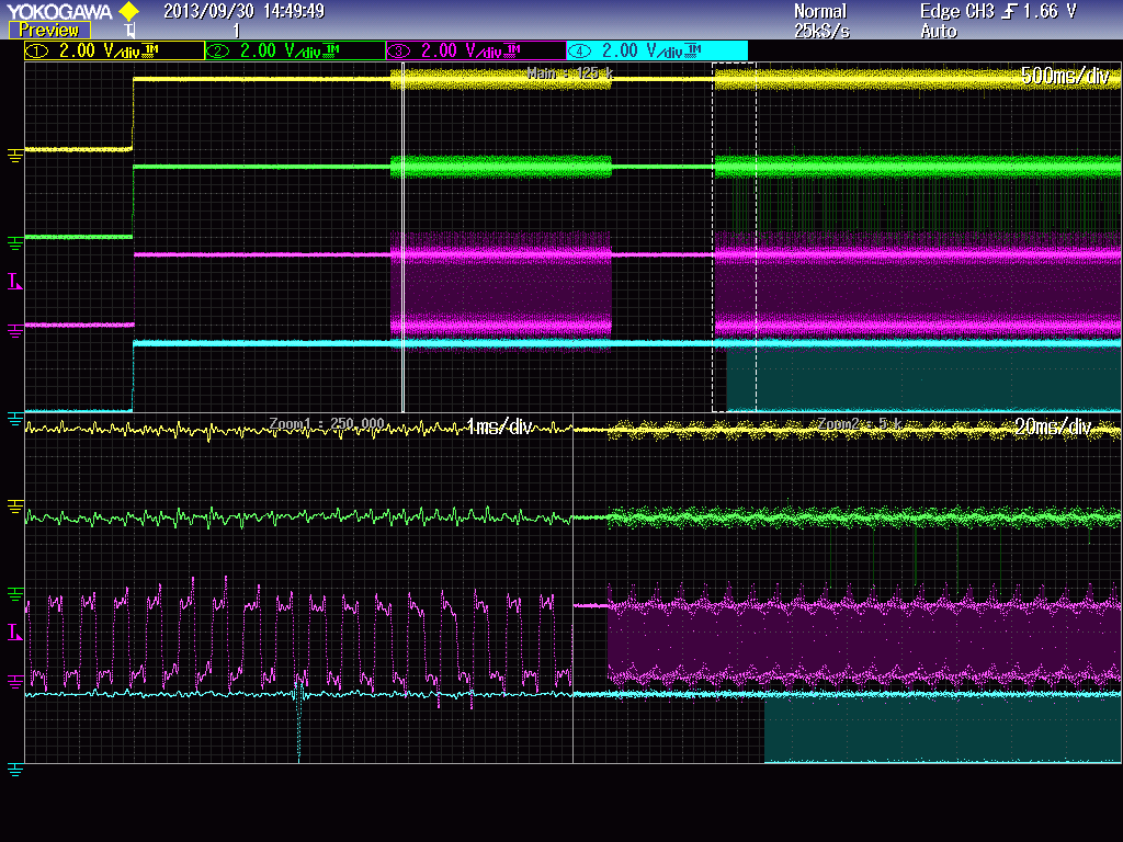
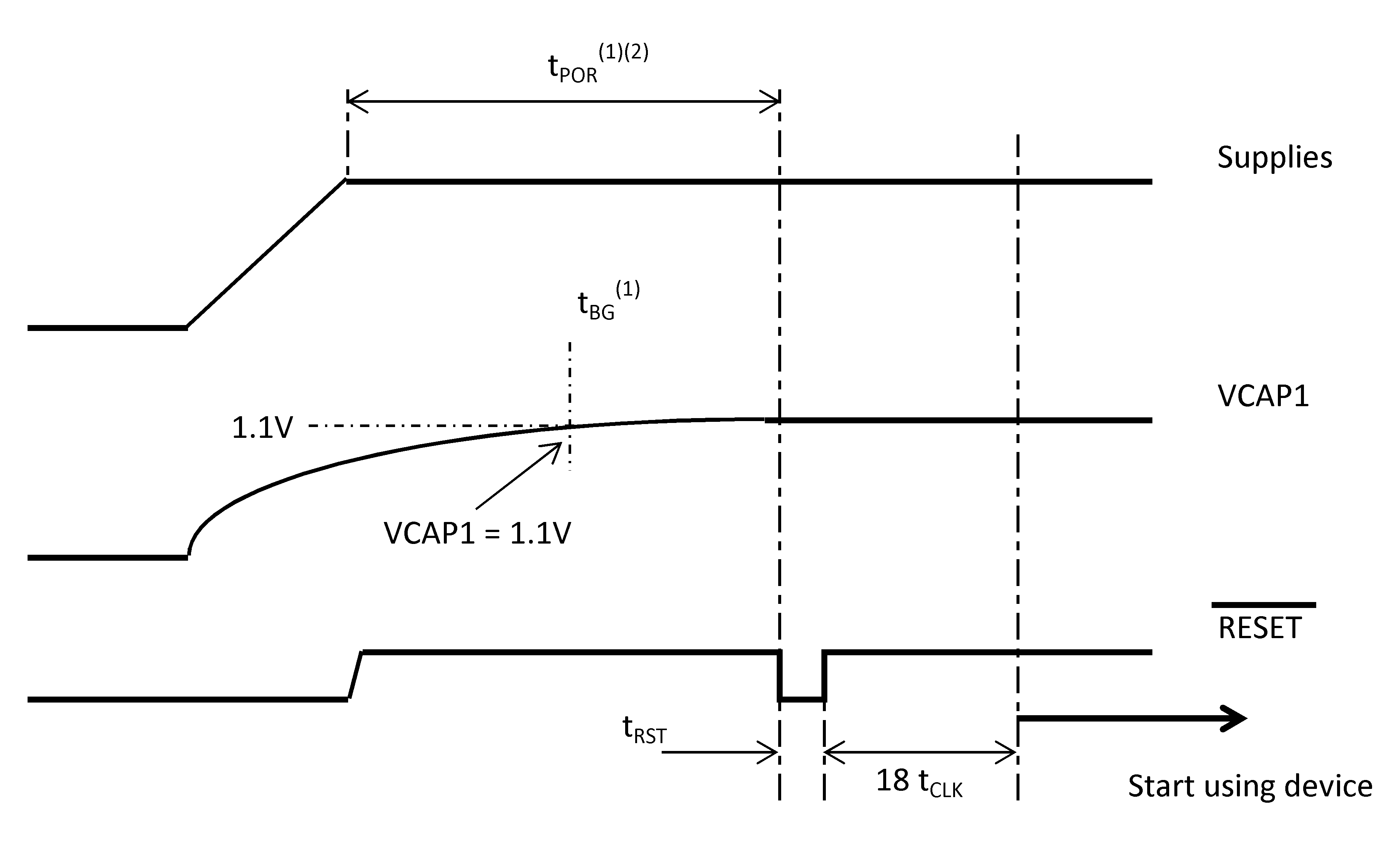
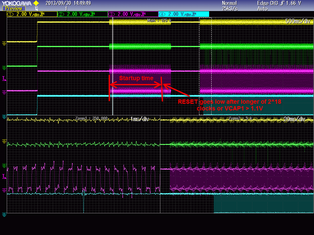
i do have a problem with a board containing multiple ADS131E06 ADC's. The board contains an FPGA, controlling 6 ADS131E06 ADC's. Each ADC has a separate SPI bus to the FPGA. In the FPGA, 6 identical SPI blocks (state machines) control the init and running of the ADC's. As the board is powered, first the FPGA is configured. After this configuration, the FPGA initializes the ADC's. The problem we're facing is that the first time the FPGA initializes the ADC's, on of the ADC's (always the same) won't work. If the FPGA is then configured again, with the same bitfile, all ADC's initialize properly. I have checked the SPI timing against datasheet timing diagrams, including power supply sequencing. I can't see any problems there. Also signals look clean and tight. I also compared the malfunctioning ADC with another ADC on the board. I can't see any timing differences there. I also checked rise-times of the power supplies, reset signals, etc. I also tried changing (lowering) the drive-strength of the FPGA . No luck there either. Do you have any suggestions or clues were to look?

Kind regards,

  • Mr Tromp  -

    • What is your power up sequence?
    • Have you reference the power-up sequence on page 51 of the datasheet?
    • What value are you using for the VCAP1 capacitance?

    In addition to the datasheet power up sequence, you might want to check the relationship between the RESET pulse low and voltage on VCAP1.  Ideally, VCAP1 voltage should be >1.1V before RESET is pulsed or 218 tclk after the supplies stabilize, whichever is longer)

    If you want to include a scope shot of your startup, we can offer some additional suggestions.

  • Hello Greg,

    1) 3V3D and 5V0A are both generated from a system supply. In practice, 3V3D rises about 25 ms after 5V0A.

    2) We did consult this diagram, according to our findings (see below) this timing is respected (with plenty margin)

    3)VCAP 1 is 22uF / 16V 1206 (X5R, AVX 1206YD226KAT2A)

    Picture 1:

    Channel 1 (yellow): 3V3 (digital supply)

    Channel 2 (Green):  5V0 (analog supply)

    Channel 3 (Magenta): Reset

    Channel 4 (Blue): VCAP1

    As can be seen, 5V0A first rises. About 25ms later, 3V3 goes up, along with the RESET.

    In this second picture, all traces except channel 4 are the same:

    Channel 4(Blue): CS

    Time between supplies and reset rising edge and first reset falling edge (Tpor) is 1230 ms (FPGA is configured during this time).

    Reset puls width is 1,8 uS.

    Time between reset inactive (rising edge) and first CS edge is 15.7 uS.

    Please let me know if you need more information.

    Kind regards,

    Laurens Tromp

  • Hello Greg,

    I have included screenshots and answers on your questions. Could you advise me further on this problem?

    Kind regards,

    Laurens Tromp

  • Are you operating from internal clock or external clock?  If external, make sure the clock is applied before you start counting the time from supplies valid to the reset pulse.

    Additionally, what does your DRDY pin do?  The device starts-up in RDATAC mode, so if everything sequences right, DRDY should start pulsing (assuming the START pin is high - might be a quick test) at the default data rate.

  • Hello Greg,

    Thanks for the reply. The device is working on an external clock, provided by the same fpga.

    In the following scope plot things should become a little bit more clear:

    In this picture, the following signals are shown:

    Channel1 (Yellow): 3V3D

    Channel2 (Green): DRDY

    Channel3 (Magenta): ADC clock (not SPI clock)

    Channel4 (Blue): Chipselect

    In the bottom half of the picture, two zooms are shown, from the first and second attempt to read the ADC data.

    As you can see, the first time, there is a CS pulse, indicating communication is performed. I have checked this actually happens, at this scale it is a little bit hard to see because of the undersampling. The second attempt to use the ADC succeeds, as shown in zoom2. In both cases, about 55 ms difference is found between the start of the system clock and the first SPI command. The ADS131E06 does not seem to start in RDATAC mode. Could this indicate the source of this problem? The Start pin is held low by the FPGA. This pin is tri-state during FPGA configuration and kept low as soon as the FPGA starts. In the above picture, fpga configuration takes place when the ADC clock is high and not switching. As can be seen, the FPGA is configured twice in the above picture. 

    Please let me know if you need more information.

  • The device will only start in RDATAC mode if the device powers up correctly AND START pin is high (or START command is sent).

    In the first zoom, are you expecting CS low to do something?  The device should be initialized using a low pulse on the RESET pin (not CS) at 2^18 CLK or VCAP1 > 1.1V, whichever is longer.  Make sure that the FPGA is sending CLK before you start the start-up counting. It looks like you might be counting the startup time the first time without applying the CLK to the device.  This might explain why things work the second time since the part has had enough clocks between the first and second start-ups.

    Using an external CLK, it is required for the to be present for the state machine of the device to start correctly.

    Your scope shot is marked up to show when the count should be started for the start-up wait and when RESET pulse low should occur.

  • Hello Greg,

    thank you for the quick reply.

    The start pin is always low, since the FPGA uses SPI commands to control the ADC. The startpin is wired to the FPGA so we could modify this.

    In the first zoom, the reason for showing CS instead of reset is, that on the given timescale, a 2 tclk pulse cannot be seen. Even the complete initialisation of the ADC, which are 10-20 bytes over SPI, takes place during this CS low. The reason for showing this plot is to show that both times the clk is available for 50ms before the reset is issued. After this reset, > 18 tclk (we have about 15us) is waited, then SPI communication starts.

  • Another question...

    Are you changing the frequency of the ADC clock?  It looks like in the zoomed in portion that there is a slower rate, then the clock goes high, and then a faster clock.  Maybe this is some kind of scope aliasing, but wanted to verify

  • Additionally, on the zoomed out upper portion...it shows that the ADC clock stops for a little while, a little after the previous notations showing startup time.

  • Hello Greg,

     to answe both questions:

    - The clock frequency stays the same. I suspect it is some kind of scope aliasing.

    - The fact that the ADC clocks stops is correct. Currently, we do reconfigure the FPGA using the same bitcode, which is basically a fancy way initializing the ADC twice.

    As told in the opening post, the ADC does not start the first time it is initialized, but the second time it does. Meanwhile, as far as I can see, al timing is equal. In some way, this is no surprise, since the same FPGA code is loaded and executed again. I do beliefe, the AD converter gets somehow in a strange mode, when we start the board. The first initialization of the ADC fails, because the ADC is in this strange mode. After reconfiguration of the FPGA, the ADC is reset again, and works. The problem though is to find what makes the ADC go into this strange mode.

  • Mr Tromp -

    What is the "strange mode" that you describe?  Behavior?

    Can you verify the timing as shown below?  If the device is working the second time, it sounds like an incorrect initialization/not enough wait time the first start-up.

    Note 1:  Reset should occur after VCAP1 >1.1V OR tPOR = 218 tclk, whichever value is LARGER.
    Note 2: For external clocking, tPOR is valid beginning at the time when CLK is present AND supplies are stable.

  • Hello Greg,

    Thanks for your quick reply.

    the "strange mode I describe is the behaviour during the first initialization attempt. The behaviour is that the ADC does not respond to SPI communication. Exactly the same commands with the same timing as the succesfull second attempt are sent to the ADC.

    Vcap reaches 1.1V 600 ms after power up. It taks about 1200 ms after power up before reset is asserted. Fclk = 2,048 MHz, so 2^18Tclk= 128 ms.

    Kind regards,

    Laurens

  • Hello Greg,

    do you have any suggestions on what to check / measure next?

    Kind regards.

    Laurens Tromp

  • As a level set/double check for ADC startup:

    1. Power up supplies...AVDD, AVDD1, and DVDD

    2. Apply external clock.

    3. Wait 2^18 clocks or until VCAP1 > 1,1V.  Issue the RESET command.

    3(optional test). If you raised START pin, device should begin to pulse DRDY at default datarate and default settings.

    4. For communication via SPI , send SDATAC to device to stop RDATAC mode.  If device was converting, DRDY will stop.

    5. Configure device/send commands as required.

    ----------------------------

    If the device isn't responding after power-up, make sure you send SDATAC before sending any commands or register read/writes.  Otherwise, the part may ignore any communication.  Step 3 in above is a quick check in that once the device powers up, if you raise START pin, it should start pulsing DRDY (at default settings).  If you don't see this without anything further, we may need to investigate the connections or future debug.

    If you still have problems, can you send either a schematic of your hardware or block diagram with connections, so that we can make sure everything is OK.

  • Hello Greg,

    thank you for your reply. One of our VHDL-engineers will make a version of the firmware that keeps the START pin high. I expect this firmware version early next week. If you can provide me your emailadres I will send the schematics to you.

    Kind regards,

    Laurens Tromp

  • Mr Tromp -

    You can send the schematics to pa_deltasigma_apps (at) ti.com (replace "(at)" with "@")

  • Hello Greg,

    i've sent a copy of the relevant schematics to the emailadres mentioned. I've also received the modified firmware version, which has 2 changes in comparison to the code used before:

    - Start pin is kept high

    - Time between ADC reset pulse and first communication from 50 ms to 250 ms.

    If this is done, as soon as the ADC is reset it starts toggling DRDY at 16 kHz, which indicates setting the ADC using SPI is completed succesfully (default datarate is 32 kHz). I will see what happens if the extra delay is removed, this will indicate which change has solved the issue.

    Can you indicate why the part does not start up when the start pin is kept low? According to the datasheet this should be working.

  • As per the datasheet, the part requires that you start conversion, either by pulling START pin high OR sending the START command (see Data Ready section,pg 26 and START section, pg 28)

  • Hello Greg,

    sorry for the delay, I have been busy on other projects. As said earlier, we use the start command over the serial interface to start the ADC. As indicated before, keeping the start pin high and increasing the delay between reset and first use of the device, the device reacts as expected.

    We then made two seperate firmware versions in one of which the startpin was kept high, whilst the other version only has the increased time between reset and first use. After testing these versions we concluded that the problem was not solved by pulling the start pin high, but by increasing the time between the reset pulse and the first SPI command. According to figure 49 of the datasheet this should be 18 Tclk (Tclk=2,048 MHz). Increasing this time to 100 ms made the ADC react to SPI commands. A version in which this time was set to 90 us didn't fix the problem. So for some reason we must wait much longer before using the device after performing the reset, than specified in the datasheet. Is this an error in the datasheet, or are there other factors influencing this specification?

    Kind regards,

    Laurens Tromp

  • A quick recap to make sure that we are on the same point:

    1. Power up supplies of the device.
    2. Start external clock or use internal clock.
    3. Wait 218 tclk or until VCAP1 > 1.1V, whichever takes longer.
    4. Send RESET pulse (> 1tclk wide) or RESET command.
    5. Wait 18tclk before using communications with the device.

    From the description, it sounds like maybe you are still experiencing some timing issues on the initial RESET.  If the RESET command/pulse is sent too early (before condition 3 is met), the signal is ignored and therefore the extra 100ms you are waiting is the time for the part to start-up on its own.

    Let us know if this is still confusing or if things still don't work properly and we'll get you up and running.

  • Hello Greg,

    thank you for your quick reply. I agree on your recap, apart from condition 3. You say we have to wait 218  tclk. According to the datasheet (page 51) this is 216 tclk. In our design the clock runs at 2,048 MHz, so tclk = 0,488 us. In our initial fpga code we wait for ~60 ms, which is about twice tpor. If I use the 218 from your reaction (128 ms), we do not comply. Can you clarify?

    Kind regards,

    Laurens

  • Mr Tromp - 

    To clarify -
    Condition #3 was from the graphic and notes in the previous post dated 07OCT13.  This is a change in the upcoming datasheet revision and the graphic and notes in the post are what will be included.  This was to clarify start-up/power-on potential issues that have been noted for applications where the VCAP1 capacitor was designed with a large capacitance value.  When using a 22uF capacitor, most designs to not have any problems.  However, for large capacitance values, there were occasional invalid device configurations at start-up.

    These proposed changes will take into account the potential variations in the capacitance and allow for correct timing for RESET signals to be applied.

    Please let us know if you have further questions/comments.