hello,
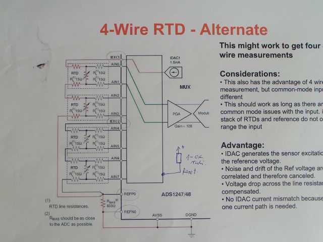
I use ADS1248 ro read 4 RTD to measure temp. (use 4 wire) see my app.2235.ADS1248.pdf
My problem is fluctuating 12 bits(LSB)!
Settings: PGA = 8
5 SPS
current 1mA
When I try ro read temp Diode inside ADS1248 flucuates 8 bits!
hello,
I use ADS1248 ro read 4 RTD to measure temp. (use 4 wire) see my app.2235.ADS1248.pdf
My problem is fluctuating 12 bits(LSB)!
Settings: PGA = 8
5 SPS
current 1mA
When I try ro read temp Diode inside ADS1248 flucuates 8 bits!