This thread has been locked.

If you have a related question, please click the "Ask a related question" button in the top right corner. The newly created question will be automatically linked to this question.

Problem in SPI communication with ADS1148 EVM

Other Parts Discussed in Thread: ADS1148, SN74LV4051A, ADS1147

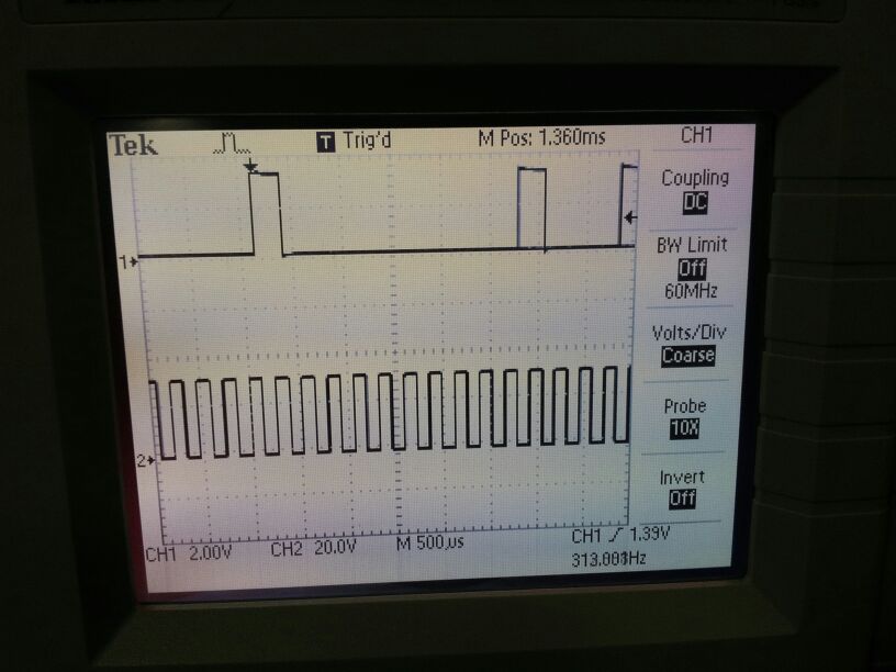
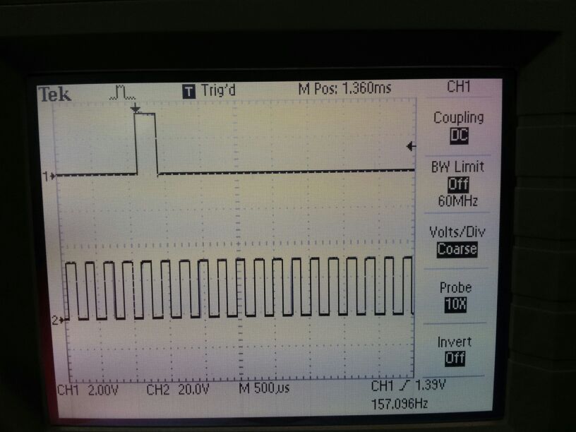
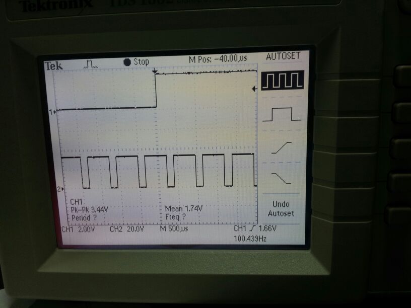
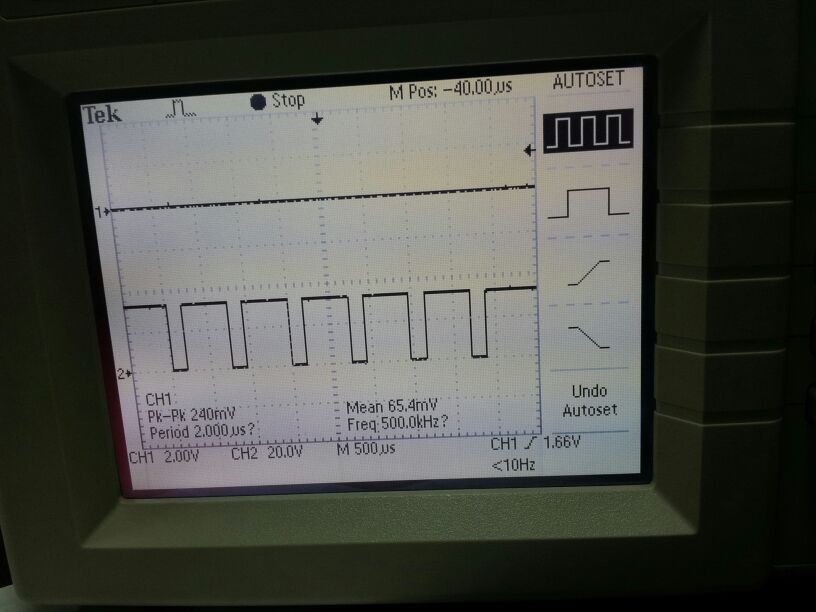
I am currently testing SPI communication in ADS1148 evaluation kit and therefore trying to read back  through SPI after sending values. I first send the SDATAC command  = 0x16 and then send the write command 0x40 and then send  0x01. I have interfaced my microcontroller(Silabs C8051f020) with the pins of ADS1148 which are CS, SCLK, DIN, DRDY, DOUT/DRDY, START and RESET. I wanted to just check the SPI communication before starting to work on reading ADC values. But I am not able to read back the values that I have sent. For example if I have sent value = 0x40,0x01 I am getting value = 0x02 in variable valcheck instead of 0x01. I have checked the signals of SPI with oscilloscope and I am able to change the clk signal as required between 0 and 3.2V. I am also sending my program which is as below:

{

ChipSelect(LOW);  //Now CS high to low indicating SPI communication enabled
STARTPIN = 1;
valcheck = ReadSPI();
WriteSPI(0x16,VALUE);
WriteSPI(0x00,COMMAND);
WriteSPI(0x01,VALUE);
valcheck = ReadSPI();

}

//////actual bit banging of SPI port in DOUT///////////
void WriteSPI(unsigned char dataout,unsigned char action)
{
unsigned char Counter;
void DelayTimer(unsigned int Delay);
unsigned char tempchar;
 //DAT_OUT = 0;
 if(action == COMMAND)
 tempchar = 0x40|dataout;
 else
 tempchar = dataout;
 //data sent for 8 bits into DATA IN line
 for(Counter=0; Counter<8; Counter++)
 {
  CY = 0;
  ACC=tempchar;
  //ACC=0xff;
  ACC = ACC << 1;
  //data to be sent is given MSB first bitwise
  DAT_IN = CY;
  tempchar=ACC;
  //delay of 1ms
  DelayTimer(10);
  //serialclock made high
  SCLK = 1;
     DelayTimer(10);
  //serial clock made low. At falling edge of clock data is taken in through DATA IN line by ADS1148
  SCLK = 0;
  //DelayTimer(100);
  //delay(1);
  //SCLK = 1;
  //delay(1);
  
    }
 DAT_IN = 0;
}

unsigned char ReadSPI(void)
{
unsigned char Counter,tempchar;
 //initially tepchar is zero. any bit to be zadded can be ored into it
 tempchar = 0;
 //initially serial clock is 0
 SCLK = 0;
 //data recieved bit wise for 8 bits
 for(Counter=0; Counter<8; Counter++)
 {
     //delay of 1ms
  DelayTimer(10);
  //serial clock made high. Data recieved on rising edge
  SCLK = 1;
  CY = 0;
  //delay of 1ms
  DelayTimer(10);
  //data recieved through DATA OUT line into carry bitwise
  CY = DAT_OUT;
  if(CY == 1)
  {
  //if cy = 1,i.e. bit recieved = 1 then put that bit in LSB
   tempchar |=1;
  }
  else
  //else keep the bit = 0
  {
   tempchar |=0;
  }
  SCLK = 0;
        //Counter value shows bit position. If bit position is less than 7 i.e. data is still to be recieved  
  if(Counter<7)
  //shift byte containing bits recieved by 1
  tempchar = tempchar << 1;
 }
 return tempchar;
}


void DelayTimer(unsigned int delay)
{
Timer1_Init(delay);
while(TF1 == 0);
TF1 = 0;
}

void ChipSelect(unsigned char state)
{
  DelayTimer(10);
  if(state == HIGH)
        CS = 1;
  else
        CS = 0;
  DelayTimer(10);
}

Please reply whether my program is OK? What else I should check or change?

  • Hi Dhiren,

    I'm not sure if I totally follow your code, the definitions and the timing.  It would be a lot easier for me to see the scope shots of the write and the read.  Can you capture the scope shots and then send them to me to evaluate?

    Thanks,

    Bob B

  • Thank you Mr. Bob for your quick response. I am attaching image(photographs since no PC facility) of my oscilloscope signals. Top signal is DIN & below signal is SCLK. I am sending 0x40 and 0x01 through DIN line. 

    Now the below signal is DOUTabove along with SCLK below. I am recieving 0x02 instead of 0x01.

    I would also like to mention that my cable length between controller and the ADS1148 EVM is about 1 feet since I am connecting the kit's connectors to my assembled PCB pin of my instrument which we are using for our other application. Please tell me where I am going wrong?

  • Hi Dhiren,

    I apologize for my delayed response as I was out of office.  If you notice, there is a difference between the two scope shots.  On the first one you see the data changing on the falling edge of SCLK and the bottom one shows the data changing on the rising edge.  The ADS1148 needs the input data to be stable on the falling edge as that is when the device latches in the data.  The same is true when you read the data with the micro, as the ADS1148 has stable data on the falling edge and changes on the rising edge of SCLK.

    Best regards,

    Bob B

  • Thank you very much, Mr.BOB. I will check the instrument again as per your advice and give feedback as per results found.

    With Best regards,

    Dhiren

  • Hello, Mr. Bob. I am again sending  my oscilloscope snaps of SPI communication. Before that I want to tell what I am actually sending and receiving.  First I send 0x16 code which is SDATAC command. Then I send 0x40 which is the write command and then 0x0f which is the no of registers = 15 to write. After this I read Data from SPI through DOUT line without sending any dummy code or NOP.  Instead of data = 15 I am getting 0 through DOUT line. I am also sending the logic flow of SCLK, DIN and DOUT line which is as below:

    Write SPI(Send Data) Procedure:

    1)      I make SCLK = 0, and then wait for 100Us

    2)      Put  data into DIN line and again wait for 100Us

    3)      I again make SCLK = 0 and again wait for 100Us. Here I expect data to be recieved by ADS1148 at falling edge of SCLK.

    4)      Then again I wait for 100Us and make SCLK = 1 and again wait for 100Us. Then I repeat  steps 2 to 7 until 1 byte of data is received. Oscilloscope snaps of send data is as below. Upper signal is Data IN line and lower signal is SCLK line.

    Read SPI(Receive Data) Procedure:

    1)      I make SCLK = 1

    2)      After delay of 100Us I make SCLK = 0

    3)      After delay of 100Us I make SCLK = 1. This is the rising edge of SCLK. I expect data to change here

    4)      After delay of 100Us I make SCLK = 0. This is the falling edge of SCLK where data should be stable

    5)      After delay of 100Us I read the 1st data from DOUT line at falling edge of SCLK.

    6)      After delay of 100Us again SCLK is made = 0 and steps 2 to 6 are repeated until 1 byte of data is read. Oscilloscope snaps of send data are as below. Upper signal is Data OUT line and lower signal is SCLK line.

    Please advice me where I am going wrong?

    Dhiren

  • Hi Dhiren,

    There are a couple of things.  First of all, you don't need all those delays.  For example, you can change the edge of SCLK to high and right away change the data out to the device.  When reading you change the edge of SCLK and then read the input pin.  When reading you only need a few nano seconds before the output of the ADS1148 is valid.

    The result of adding all the delays is that you are now violating the duty cycle requirement.  Look at the Figure 1 and table on page 12 of the datasheet.  There is a tSPWL and tSPWH requirement which means you must have a period where you cannot have a portion of the period less than 1/4 of the total SCLK period.  Try to have a 50% duty cycle where 1/2 the time the clock is high and the other 1/2 of time the clock is low.

    One observation is although it is true that there are a total of 15 registers, you probably don't want to write to all 15.  For example, you probably do not want to write to the calibration registers (0x04 through 0x09) and unless you are using the GPIO you probably don't want to write to the last three registers (0x0C through 0x0E).  In most cases you will right to the first 4 registers, and perhaps the two IDAC registers if you are using the IDACs.  This can be done in two write registers blocks.

    The actual write register command is the WREG command plus the starting register (first byte) followed by the total registers being written less one.  That means if you are going to write one register of data this byte would be 0x00, or when writing 15 registers it would be 0x0E and not 0x0F.  So the correct bytes for writing 15 registers starting at register 0 would be 0x40 0x0E.

    If writing the registers in two blocks, as I mentioned earlier, the first command is 0x40 0x03 followed by 4 bytes of data.  The next write block would be 0x4A 0x01 followed by 2 bytes of data.

    When reading back the registers the command is similar, except the RREG command is 0x20 instead of 0x40.

    Best regards,

    Bob B

  • Thank you very much Mr. BOB. Now I am able to communicate with ADS1148 and change the settings in it via changing its internal registers.I was making the mistake of not issuing the RREG command and was just expecting that the data in the output register would be same as the data sent. Now I am checking the ADC reading part.I would like to ask whether VBIAS needs to be added to AIN1 to get ADC value when input from mV source is given between AIN0 and AIN1. Also whether the following flow of code to read ADC value is correct?

    Step1: make CS low, start and reset pin high.

    Step2: Issue SDATAC command and then check DRDY for low.

    Step3: Repeatedly read ADC values by repeated issuing following commands

    i) Issue of RDATA command and wait for DRDY for low.

    ii) Get ADC value after continously reading DOUT line for 16 clock cycles.

    Please verify whether I am in the right direction?

  • Hi Dhiren,

    To read out the data in SDATAC mode, you wait for DRDY to transition from high to low, then send the RDATA command and immediately send 16 more SCLKs to retrieve the data.  When you send the RDATA command DRDY will again go high.  You must make sure that you have completed the retrieval of data before DRDY transitions again to low or the data will be corrupted.

    Best regards,

    Bob B

  • Hello Mr.BOB. Thanks for your patient support. I have successfully read resistance and mV input consecutively. Now I am reading ambient sensor after reading mV input and to do so I changed MUX1 val = 11. Then change to SDATAC mode. Then wait for DRDY to go low. Then I read the value. The code obtained is 116. This code changes to 127 if I put my finger on the chip. I wanted to know whether the code obtained is right .According to me since code for 118mV should be obtained at 25 deg and the calculted code for 2V reference should be 1933. Please suggest where am I worng?

  • Hi Dhiren,

    I'm not sure what to tell you at this point.  The system I have reads out about 1900 codes at room temp.  I tried both internal and external reference.  The only thing I can think of is either the MUX1 register is being written incorrectly or the data is being read incorrectly.

    You have stated that the MUX1 val =11, but is that decimal, binary, or hex?  If this is 11 decimal it would be totally incorrect.  If it were 0x11, then the device would be in shorted input mode with an internal short which would be closer to what you are seeing.

    Best regards,

    Bob B

  • Sorry Mr. Bob. It was my fault as I had stored my result in the wrong way. Now I am getting the value = 1906 on ambient and the value increases to 1926 after touching the IC with my finger. Thanks for your supprt. 

  • Hello Bob,

    Hello Mr.BOB, I am sending as attachment i.e. 8407.ADS1148 SCH.PDFmy schematic of ADS1148 for 32 channel  universal input DAS. Following are the details of the circuit and some query related to it:

    1)      Ports P0.2, P0.3, P0.4, P3.0, P3.1 and P3.2 re the SPI interface ports to my microcontroller. All these lines are connected to SPI interface ports of ADS1148 for 32 channel input. I wanted to know whether it is OK to connect all these lines including DRDY, START and RESETlines of 8 ADS1148 (8 x 4 = 32channel) and give it to the microcontroller.

    2)      Referring the EVM board, I have connected BAT54 between AVss and AGND and also between REFP0 and AVdd. Also 5.1V Zener connected to REFP0.

    3)      Resistors R11 to R14 and C20 to C25 are for filtering the inputs along with torroidal.

    4)      SW1 is to select input for 4-20mA.

    5)      I have given 2.5V zener to REFP1.

    6)      Also Capacitors C15 to C17 = 10UF(non polarized) were added after referring the EVM.

    7)      For filtering of reference (REFP0, REFP1) resistors R21, R22, C26, C27 and C28 are after referring application report SBAA201.

    8)      Resistance R23 is Rbias for RTD input.

    9)      Power supply section , U7 and J10 is part of my circuit which would change depending on my application . At present it just gives the required 3.4V or 5V required for the ADS1148 circuit.


    Please check whether the circuit is OK or whether some modifications are required since we are making our 1st prototype using ADS1148.

  • HI Dhiren,

    See my comments and answers below marked in red.

    Best regards,

    Bob B

    Dhiren Shetty said:

    Hello Bob,

    Hello Mr.BOB, I am sending as attachment i.e. 8407.ADS1148 SCH.PDFmy schematic of ADS1148 for 32 channel  universal input DAS. Following are the details of the circuit and some query related to it:

    1)      Ports P0.2, P0.3, P0.4, P3.0, P3.1 and P3.2 re the SPI interface ports to my microcontroller. All these lines are connected to SPI interface ports of ADS1148 for 32 channel input. I wanted to know whether it is OK to connect all these lines including DRDY, START and RESETlines of 8 ADS1148 (8 x 4 = 32channel) and give it to the microcontroller.

    BB> DRDY, and DOUT/DRDY are output pins.  DRDY is never tri-stated and because CS is tied low, DOUT/DRDY is not tri-stated either.  You cannot connect these pins directly together.

    2)      Referring the EVM board, I have connected BAT54 between AVss and AGND and also between REFP0 and AVdd. Also 5.1V Zener connected to REFP0.

    BB> I think you misunderstood the meaning behind the zener and the protection diodes.  These were added to the EVM for a couple of reasons.  The first is the EVM can use single suppy or bipolar supplies (+/-2.5V).  This means standard connections to ground might damage the device if switching between supply modes.  The second reason is for overvoltage protection from adding external reference supplies to the EVM with incorrect references to ground.

    Your implementation is incorrect, and as this is a system design and not an evaluation platform, there is no need to add these components.  AVSS must connect directly to analog ground.  Remove D4, D5 and Z2.

    3)      Resistors R11 to R14 and C20 to C25 are for filtering the inputs along with torroidal.

    BB> Your resistor values are quite large (68k).  You may have some bias current issues with voltage drops across these resistors, so after testing you may have to lower these values and increase cap values to maintain the same cutoff frequency.  Also, the differential caps C20 and C21 must be at least 10 times larger than C22-C25 to limit the effects of drift.  You want the differential cap to dominate so that common mode RC filter does not create differential voltages. 

    4)      SW1 is to select input for 4-20mA.

    5)      I have given 2.5V zener to REFP1.

    BB> Be careful here making sure the voltage remains stable and is low noise.

    6)      Also Capacitors C15 to C17 = 10UF(non polarized) were added after referring the EVM.

    7)      For filtering of reference (REFP0, REFP1) resistors R21, R22, C26, C27 and C28 are after referring application report SBAA201.

    BB> Same response as point 3 above.

    8)      Resistance R23 is Rbias for RTD input.

    BB> R23 needs a direct connection to ground (at R23-R22 connection).

    9)      Power supply section , U7 and J10 is part of my circuit which would change depending on my application . At present it just gives the required 3.4V or 5V required for the ADS1148 circuit.

     BB> I do not understand how your power supply is supposed to work.  You have 68k ohm resistors in each ground leg and U5 is connected directly to GND.  You should revisit the current paths.

    Please check whether the circuit is OK or whether some modifications are required since we are making our 1st prototype using ADS1148.

  • Hello Mr.BOB. Thank you for your support.  It has been really helpful in implementing our circuit faster for our prototype.  As per your recommendations I have made the necessary changes in the overall block diagram scheme of 32 channel data logger as shown3821.ADS1148_SCHEME_32chLOGGER.pdf I had also changed the power supply section which was my error. Still I have some queries:

    a)      For 32 channel data acquisition, I have used 8 ADS1148. Since SCK, DIN and START pins are multiplexed only 3 ports are used for them. But since DOUT/DRDY, CS and DRDY are not multiplexed(short together), I need 24 extra port lines of microcontroller for them. How can I reduce these port lines?

    b)      Whether DOUT line can be multiplexed as in usual standard SPI configuration MISO(for microcontroller) is multiplexed?

    c)       I feel that I would be using internal reference and remove external reference of 2.5V which was given to REFP1 which I think would be better. I will retain the capacitor of 10UF between REFP1 and REFN1.

    Regards,

    Dhiren

  • Hi Dhiren,

    Please see my comments in red below.

    Best regards,
    Bob B

    Dhiren Shetty said:

    Hello Mr.BOB. Thank you for your support.  It has been really helpful in implementing our circuit faster for our prototype.  As per your recommendations I have made the necessary changes in the overall block diagram scheme of 32 channel data logger as shown3821.ADS1148_SCHEME_32chLOGGER.pdf I had also changed the power supply section which was my error. Still I have some queries:

    a)      For 32 channel data acquisition, I have used 8 ADS1148. Since SCK, DIN and START pins are multiplexed only 3 ports are used for them. But since DOUT/DRDY, CS and DRDY are not multiplexed(short together), I need 24 extra port lines of microcontroller for them. How can I reduce these port lines?

    BB> There are not many options for CS, but when you use CS you can tie all the DOUTs directly together as the outputs are tri-stated when CS is high.  At this point you are at 9 inputs (8 CS + 1 DOUT) with 8 DRDY inputs (24 to 17).  To reduce the CS to three lines from the micro you could use a demultiplexer (3 to 8) such as the SN74LV4051A.

    b)      Whether DOUT line can be multiplexed as in usual standard SPI configuration MISO(for microcontroller) is multiplexed?

    BB> Again, you can tie the DOUTs directly together if ADS1148 devices are controlled by CS.

    c)       I feel that I would be using internal reference and remove external reference of 2.5V which was given to REFP1 which I think would be better. I will retain the capacitor of 10UF between REFP1 and REFN1.

    BB> Your reference requirement will depend on the full-scale range necessary for your design.

    Regards,

    Dhiren

  • Hello Mr.BOB. Thank you again for your support.  As per your recommendations I have made the necessary changes.

    Again I am sending my 32 channel scheme4628.ADS1148_SCHEME_LOGGER1.pdf after making some changes. I have also added RESET line which was not added previously. Please check whether this scheme is OK.

    Regards,

    Dhiren

  • Hello Mr.BOB. Thank you again for your support. As per your recommendations I have made the necessary changes. Again I am sending my 32 channel scheme 1157.ADS1148_SCHEME_LOGGER1.pdfafter making some changes. I have also added RESET line which was not added previously. Please check whether this scheme is OK. Regards, Dhiren

  • Hi Dhiren,

    That scheme should work.  Keep in mind that the state of CS will be dependent on the state of the demultiplexer.  A couple of options would be to place pullups or pulldowns on the address inputs (to create a default condition), or pullups on the ADS1148 CS pins with another control line to the demultiplexer to disable the output.  I prefer the latter option so that I can completely disable the outputs of the demultiplexer so all CS will be high when not communicating to the devices.

    Best regards,

    Bob B

  • Hello Mr.BOB. Thank you again for your support.  I will be implementing the recommendations in the prototype.

    Regards,

    Dhiren

  • Hello Mr.BOB. I have 1 more  query related to PCB designing of ADS1148.

    We are working on a single PCB for ADS1148 for 32 channels. My microcontroller would be on another PCB. The track length between ADS1148 and my microcontroller could be upto 20cm(200mm).  There would also be a connector between ADS1148 and microcontroller PCB. I wanted to know whether this length of track could cause problem in SPI communication. If yes what could be the possible solution to it?

    Regards,

    Dhiren


  • Hi Dhiren,

    You need to be careful with capacitance and inductance of the cabling.  Usually a ribbon cable will work well when each connection alternates with ground.  That would be signal, ground, signal, ground, etc..  This allows for good signal return paths and reduces the effect of external noise.  High frequencies clocks may have issues (100MHz) but at 2MHz this should be ok.

    Best regards,

    Bob B

  • Hello Mr.BOB.

    I am currently testing ADS1147 in my new PCB. During testing for the thermocouple input, I gave mV input to ADS1147 from mV source. For mV input I configured ADS1148 as follows:

    1) MUX selection for channel 1(MUX0 = 0x01) or channel2(MUX0 = 0x13)

    2) VBias selection for channel 1(Vbias = 0x02) or channel2(Vbias = 0x08)

    3) MUX1 selection for reference(MUX1 = 0x30) i.e. internal reference ON and onboard reference selected.

    4) SYS0 selection for PGA(SYS0 = 0x50) i.e.PGA gain set for 32

    5) IDAC0 = 0x00 and IDAC0 = 0xff as no current source is selected.

    I have observed that when VBias is selected = 0x02/0x08, the ADC code changes as per PGA gain selected but when Vbias = 0x00 the ADC code changes as per PGA =1 and not as per set PGA. Is it necessary to add Vbias to negative input(AIN1 or AIN3) because without Vbias the ADC code obtained is very less i.e 1000 to 2000 counts for any set PGA..

    Regards, Dhiren

  • Hi Dhiren,

    Yes you must bias the sensor into the correct common mode input range for the gain setting used either by an external bias (resistor divider for example) or by using the VBIAS.  A floating input could float to any value, including floating toward the supply rails.  If this happens then you will be outside the common mode range for the ADS1147.

    VBIAS was added to the ADS1147 for biasing a floating sensor to mid-supply of AVDD so that the sensor will be measured for the correct common mode. 

    Best regards,

    Bob B

  • Hello Mr.BOB. Thank you for your support. I have one more  query

    I connected 4-20mA input from my mA source to the input (terminal T1 terminal no 2 and 3) of my circuit as shown in circuit diagram attached6523.8407.ADS1148 SCH.pdf and turn SW1 on so that voltage across resistor R9  is given to ADS1148 input. I have found that I am getting non linear ADC result for different  mA levels in 4 – 20mA range. 4 – 20mA is converted to mV by the resistor R9 = 51E as shown in the attached diagram. I also shorted the series resistors R11 and R12.

    The ADC codes obtained are as follows formV input given to ADS1147:

    185mV                                    ADC result = 16B9

    372mV                                    ADC result  = 2F2C

    560mV                                    ADC result = 4961

    750mV                                   ADC result = 6615

    The ADC result for thermocouple input for the same configuration as mentioned in my previous mail was found to be OK. For 4-20mA input the configuration is as follows:

    1) MUX selection for channel 1(MUX0 = 0x01) or

    2) VBias selection for channel 1(Vbias = 0x02)

    3) MUX1 selection for reference(MUX1 = 0x30) i.e. internal reference ON and onboard reference selected.

    4) SYS0 selection for PGA(SYS0 = 0x60) i.e.PGA gain set for 32

    5) IDAC0 = 0x00 and IDAC0 = 0xff as no current source is selected.

    Please suggest where I am wrong. 

    Regards,

    Dhiren


  • Hi Dhiren,

    The data given does not line up well with respect to the register settings.  What are the voltages you are giving me?  Are they measured or calculated?  Also, the SYS0 register setting doesn't match for a gain of 32. 0x60 is actually a gain of 64.

    If the shunt resistor is 51 ohms, and the current can range from 4mA to 20mA, the range of voltage that can be dropped across the resistor will be from about 200mV to about 1V.  This would mean that with a 2.048V reference the most gain that could be applied is a gain of 2.  The LSB size would be 2.048/2/(2^15-1), or about 31.25uV.

    If you were expecting 185mV I calculate 181.78mV for a gain of 2, so I think that there may be a mistake in the register settings you sent me.  From the results, assuming I'm calculating correctly based on what I think the settings really are, the trend is forcing the measured voltage higher as current is increased. I think what may be happening is an added voltage drop occurs across the input filter resistor through VBIAS to ground.  1uA through this path would create the difference you see.  If this is happening you should be able to measure a voltage drop across resistor R12 of about 68mV.

    Using large input resistor values can affect the measurement as there will be an input bias current.  Even though this current is small, using large value resistors will show some error.  Also, I see that the differential cap value is the same as the common mode cap value.  If there is any mismatch to the filters (either by tolerance or drift), a difference voltage can be created also adding to error.  This could also be a part of the problem you are seeing.  For example, C20 should be at least 10 times larger in value of capacitance as compared to C22 and C23.

    Please verify the exact register settings used and how your are determing the expected voltage.  It might be more helpful to know the value of current being applied.  Also send me the code returned for the shorted input condition.

    Best regards,

    Bob B

  • Hello Mr.BOB. Thank you again for your support. I admit there was a mistake. The gain was of 2 which you correctly identified. I have tested the circuit after shorting the resistors R11 and R12 and removing the capacitors C22,C23 and C20. It is virtually connecting the mV input from resistor R9 directly to the input pins of ADS1148. I again connected 4-20mA input from my mA source to the input (terminal T1 terminal no 2 and 3) of my circuit as shown in circuit diagram attached6523.8407.ADS1148 SCH.pdf and turn SW1 on so that voltage across resistor R9  is given to ADS1148input. Even without series input filter resistors and capacitors I have found that I am still getting non linear ADC result for different  mA levels in 4 – 20mA range. 4 – 20mA is converted to mV by the resistor R9 = 51E as shown in the attached diagram. I also shorted the series resistors R11 and R12.

    The ADC codes obtained are similar as before. For 4-20mA input the actual configuration is as follows:

    1) MUX selection for channel 1(MUX0 = 0x01) or

    2) VBias selection for channel 1(Vbias = 0x02)

    3) MUX1 selection for reference(MUX1 = 0x30) i.e. internal reference ON and onboard reference selected.

    4) SYS0 selection for PGA(SYS0 = 0x10) i.e.PGA gain set for 2

    5) IDAC0 = 0x00 and IDAC0 = 0xff as no current source is selected.

    Again please suggest where I am wrong even though  I feel there is nothing in the circuit to go wrong except if there is any problem in the PCB. 

    Regards,

    Dhiren

  • Hi Dhiren,

    This seems straightforward to me, and you should see better results.  The only thing I can think of at the moment is a leakage current path through the VBIAS circuit where your source current supply may be leaking through to AVSS (like maybe a ground loop).  I will attempt to set up a similar circuit in the lab as soon as I can to verify and observe the operation using your configuration.

    Best regards,

    Bob B


  • Hello Mr.BOB. Thank you for your support. I have to admit there was a mistake from my side. I had kept the current source ON while  I was changing between 2 channels . I kept current source ON in the 2nd channel for the 1st channel.

    The current source had its effect on the result. I am extremely sorry as I had mentioned earlier that the setting for cuurent source was OFF but I had not exactly checked what I had done for the second channel as I had ignored the result of the second channel.  I had checked the result without the filter resistors and capacitors and they are OK. I would recheck them with the filter resistors and capacitors.

    Regards,

    Dhiren


  • Hello Mr.BOB. I am testing RTD input with ADS1147  in my PCB and I have found that there is fluctuation of 5 degrees. This reduces to 1degree as soon as I connect JTAG Connection(JTAG provided on PCB to program microcontroller) to my USB adaptor which is connected to USB of my computer. I then observed that if I connect only my gnd pin of JTAG connector of USB adaptor the fluctuation remains for 1dregree. The fluctuation of 5degrees reappears as soon as I disconnect USB adaptor from the P.C. I have checked both 5V AVDD and VBIAS 2.95 and they are stable w.r.t. AGND. Please suggest how to solve this problem.

    Regards,

    Dhiren

  • Hi Dhiren,

    I think you have pretty much answered your own question.  If the USB ground is affecting the measurement, then you have some sort of instability with noise relative to ground.  Remember that "ground" is a reference point but is also a part of the system.  Ground bounce, or some other distburance to ground can not only affect the measurement but the integrity of the power system as well.  If you route "ground" with traces, you can pick up noise on the ground as well as you can on any other input.  Sometimes the noise can come from the external supply routing, such as a wire from the supply to a connector on the PCB.  So, before you can solve the problem you have to identify the source of the problem.  I've given you a couple of ideas of places to look.  Another thing to consider is what is happening when you connect the USB ground.  Does it make an earth ground connection that is missing from your power source?

    Best regards,

    Bob B