This thread has been locked.

If you have a related question, please click the "Ask a related question" button in the top right corner. The newly created question will be automatically linked to this question.

ADS1282 layout checking

Other Parts Discussed in Thread: ADS1282, OPA1632

Dear Sir,

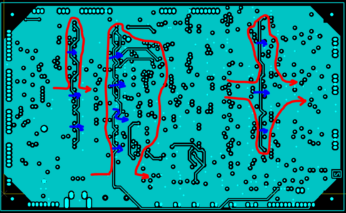
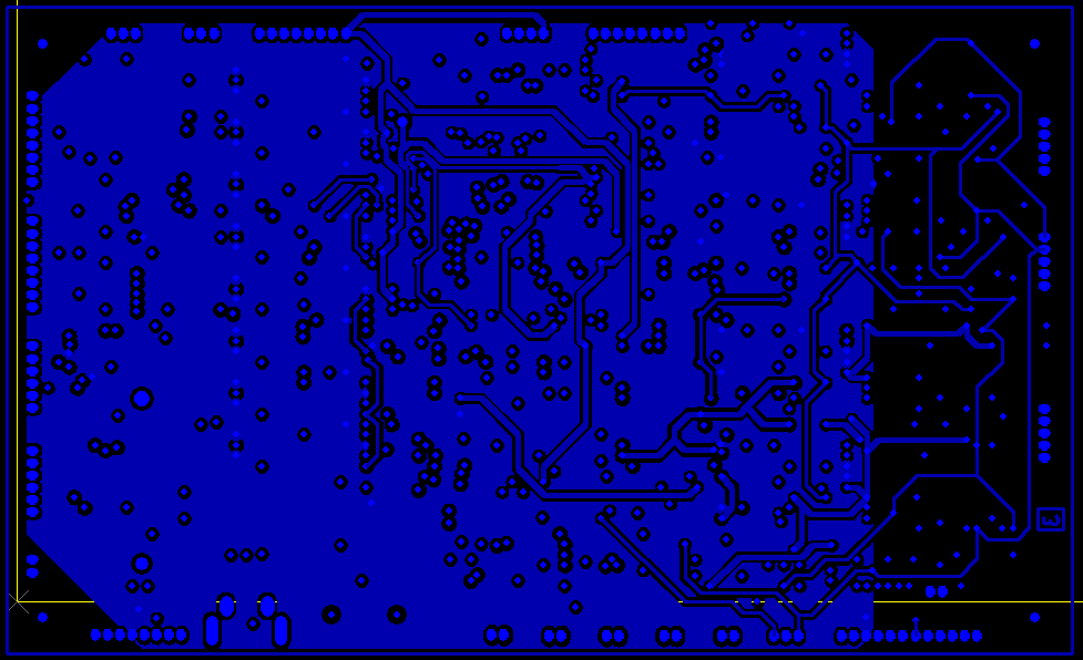
I have attached schematic of adc portion, and gerber file for verifying from you whether the layout is ok or not. So please can you verify the same. Four ads1282 is used.  SPI multiplexing is done to communicate with the CPU. 

Please can you verify the same.

Gopal Rao.

schematic of adc.pdf
  • Hello Gopal,

    Please refer to my schematic review notes below:

    • I noticed the R7 and R8 resistors (as well as R40, R41, R62, R63, R86, & R87) which appear to bias the ADS1282 PGA outputs to AVSS and +5Vref, respectively. I have not seen this kind of connection used before and am interested if there is a need for it? The ADS1282 PGA inputs are properly biased; therefore, I would expect these resistors are only contributing thermal noise (and coupling other noise sources) to the sampled signal voltage.

    • I see that the SPI multiplexing gates both SCLK and DIN. This is not a problem, but this can be simplified to only gate SCLK. Refer to my post on the following thread for an example: http://e2e.ti.com/support/data_converters/precision_data_converters/f/73/p/291510/1018745.aspx#1018745

    • Inductors L1, L2, L3 & L4 are probably okay for filtering the digital supply. However, digital circuits tend to be inherently immune to noise so I don't see much benefit. Double check, that the digital supply source can sink current in the case of a transient current event!

    • I may recommend removing AVDD2 and just using AVDD1 in it's place. AVDD2 only seems to be used for biasing some of the ESD diodes and inputs on ADC channels 3 & 4. It is hard to see from the schematic how this connection may affect the circuit and the various return currents. My concern is that having some circuits reference both AVDD1 and AVDD2 may greatly increase the return current loops and cause return currents from both supplies to interact. This interaction may increase supply noise and degrade the ADC performance.

    • There are independent references for each ADC channel reference and op amp reference. I think all OPA1632's could share a reference without any issues. The ADS1282's could also share a single REF5050 if the reference was buffered to each ADC to prevent reference cross-talk. This is just an alternative design option.

    I did not observe any functional problems with the schematic. I recommend paying close attention to return currents while designing the layout to minimize return current loops for achieving the best noise performance and immunity.

    It was a pleasure to review your schematic!

    Best Regards,
    Chris

  • Dear Chris,

    Thanks for your valuable feedback on the issues. You are right that R7,R8,etc are not needed, it is I overlooked some of my earlier design and incorporated it here.  

    Also I can get rid of one multiplexer by not multiplexing DIN.

    Regarding AVDD1 and AVDD2, I thought it will be better so as to reduce power supply noise.  But as it will cause ground loop problems, i will get rid of two power supply. 

    Independent references are there only to reduce cross talk. 

    I will do the necessary changes, as detailed by you. 

    Can you verify the Gerber file. It is 4 layer PCB. 

    Thanks

    Gopal Rao.

  • Hi Gopal,

    Your welcome! I'd be glad to review your Gerber files too!

    Best Regards,
    Chris

  • Dear Chris,

    Attached herewith is Gerber file.  

    Also attached is power supply  circuit.  Can you verify this also. As you told me to double check the digital supply source can sink current in case a transient current requirement.

    Regards

    Gopal.


    Gopal.zip
  • Hi Gopal,

    The first thing I looked at was your ground plane and I noticed that you have traces in this layer. The problem with these traces is that they block the flow of return current. Any current that is trying to flow in the path of least inductance below it's signal trace will be re-routed around the traces in the ground plane (see my annotation below). This greatly increases the return current loop area and will introduce parasitic antennas on your PCB. This is probably the #1 cause of noise and EMC problems with PCB layouts. If you can remove these long traces from the ground plane you will see a difference!

    I know your board is crowded, but at the very least you need to reduce these current loops by providing multiple alternative paths to current to flow (for example, where I've shown blue arrows). A better solution is to ensure that no trace blocks the return current path. The best implementation would be to have no traces breaking up the ground plane (traces around the outside of the board don't break up the ground plane, but they can be more susceptible to noise pick-up from external sources).

    The same principles also apply to the plane on the VCC layer.

    Here are some additional and minor things I noticed:

    • Minimize the trace lengths that connect the PGA differential filter cap to CAPP and CAPN pins on ALL ADS1282's. Remember to remove the connecting resistors (R7, R8, etc...)


    • Connect these two DGND nets (under U6) on the top layer to decrease impedance to DGND. I think you can shift the via to the right to make this connection.

    I also have a question about the ground connections I noticed on the schematics...


    When you tie these ground nets together are you making a single point connection or are you using the same ground plane for both of these nets? I recommend the latter option as it usually reduces the return current loop area and/or it creates a lower impedance connection to ground.

    Best Regards,
    Chris