This thread has been locked.

If you have a related question, please click the "Ask a related question" button in the top right corner. The newly created question will be automatically linked to this question.

DAC161S997 Grounding and EVM Component Question

Other Parts Discussed in Thread: DAC161S997, DAC161S997EVM, DAC161P997

Hello,


I am using the DAC161S997 to create an analog control signa that loads the device anywhere from 4-20mA out the output. This signal is used to control a load that may or may not have a common ground with the transmitter.


I think I have run into a problem with my implementation. I would like to have loop power on our board but with the way COMA and OUT are configured, it looks like I would actually need a floating/isolated power supply on board for the loop power.


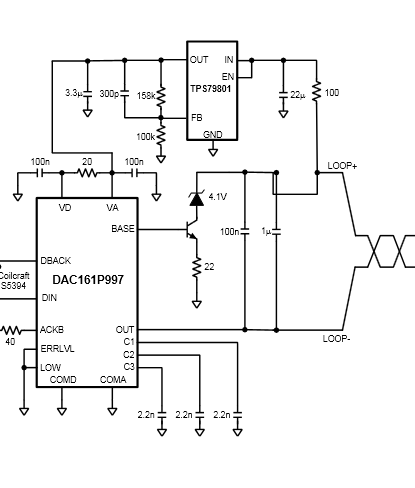
The first two figures of the datasheet (SNAS621 –JUNE 2013) show the emitter resistor connected to local ground and the OUT pin (Loop-) connected to the loop (external) ground and it looks like COMD & COMA are connected inside the IC by a 40 ohm resistor.   (Fig 9 & 10)

So I would need to place the loop receiver resistor (nominally 250 ohm) between OUT and the ground of the loop power supply.   This would raise the OUT pin up by as much as 5V (@20mA not account for wiring).


As a separate question the eval board has a 3.9V Zener (D1) inline with the transistor.  What is the purpose of this zener?  The datasheet never shows/discusses this diode.


Thank you for your help.


Ryan May

  • Maybe we could back up one step farther.

    The drawings are very poor at showing the ground paths. 

    Each drawing shows an LDO - with out a ground. DAC161S997EVM the pdf has the power supply section chopped out of it.

    The modules (IC DAC161s997) has a triangle ground pin - with no real world ground ref.

    It looks like the current to operate the DAC - returns via the 4-20ma line  - correct?

    OR

    Does the LDO reference real world ground - and the inside of the dac floats ?

    Then why in the functional diagram on page 2 - is the micro on the DAC floating ground.

    Does someone have a circuit diagram that is complete?

    Carl

  • Hello.

    The system block diagrams unfortunately do not show the LDO connection to COMA/COMD for powering the local circuitry.

    It is not recommended to place an external resistor between the COMD/COMA (local ground) and the Out pin (Loop-), as this would affect the DAC161S997's performance.

    The DAC161S997 uses the zener to detect the loop error condition, which is when the loop supply voltage drops too low. The DAC161S997 detects this condition when the output transistor saturates. The zener increases the transistor saturation voltage to be above the DAC161S997 VA/VD minimum.

  • This is what I want to do - 

    The system block diagrams unfortunately do not show the LDO connection to COMA/COMD for powering the local circuitry.

    Are there any diagrams?

    Thanks

    Carl

  • The loop interface of the DAC161S997 is similar to the DAC161P997; you can refer to page 28 of the DAC161P997 datasheet (http://www.ti.com/lit/ds/symlink/dac161p997.pdf) for some additional information on how the LDO should be connected. I have attached the relevant image from the datasheet below.


  • Hi

    What is pictured  - is a two wire circuit - in which ALL CURRENT returns via the LOOP- path.

    There cannot be any load - in the circuit - micro - device - that returns current that does not travel down Loop-

    Thanks - but it is still extremely unclear " none of the references show a complete ground circuit.

    But what if I want a 3 wire device - LOOP+ LOOP- Ground.

    So that a load is on the circuit - Its current would not return via loop - but via ground.

    The issue is the above schematic - the DAC is isolated. but in the SPI dac - it cannot be isolated.

    It micro must share ground with the DAC- and the thing the micro is talking to - to get the data - that is's SPI'ing

    must share a ground.  

    So all the ground info is very important - and missing -  

    OR

    Must the Micro - and its load be on another ground - thus requiring that the SPI be isolated - is so

    Also - why is there a 100 ohm resistor in the Vreg supply

    thanks 

    Carl

    .

  • The problem that I am trying to get answered is how the Loop- is connected to the system ground. Can this be shorted?


    Otherwise will I need an islolated supply between the DAC and the points I am sensing.

    A quick answer would be appreciated.


    Ryan May

  • Hi Ryan.

    The 4-20mA loop reports a measurement as an analog current. The DAC161s997 and DAC161p997 are DACs that control the loop current with a 16bit resolution. The dac161s997 is a very low power device, and is intended to use the power from the loop to operate. One of the things that the dac161s997 does is define a local ground. This local ground needs to be isolated from the loop-, otherwise the dac161s997 will not be able to control the loop current. There may be some designs where the local ground of the dac161s997 can be the same as the system ground, but in general it is better that the dac161s997 local ground not be connected to system ground. 

    In some configurations, the loop- is connected to system ground. This is acceptable, as long as the dac161s997's local ground is not also connected to the system ground.

    Regards,

    Chris O


  • Hi

    I am getting there, although my design does not work

    I can talk to the DAC - see the SPI data - yet I am always in current error. 

    What is the purpose of the Zener in the transistor circuit - this does not show up un the data sheets.?

    I have loaded the DAC161S997EVM software on 4 computers. XP and Windows 7 - It does not work on any of them I was going to look at the signals on the EVM and the data traffic and compare it to mine.

    I have a call into tech support on this - any idea? The software cannot find the COM port.

    Carl 

  • Sorry - missed this

    The DAC161S997 uses the zener to detect the loop error condition, which is when the loop supply voltage drops too low. The DAC161S997 detects this condition when the output transistor saturates. The zener increases the transistor saturation voltage to be above the DAC161S997 VA/VD minimum.

    Question - Is the zener necessary for operation?

    Carl

  • Never mind - that is what we thought - it stops transistor operation when incoming voltage is below VREG output.

    It just improves low end voltage operation. 

  • Try downloading and installing the following driver (ni-visa 5.4) from National Instruments Web Site: 

    http://www.ni.com/download/ for your operating system. It seems that some drivers are missing from the TI software installation package.

  • HI  Chris

    In the DAC161S997 datasheet, on page 22, Figure 22, where the triangle ground come from?

    When I power the circuit that the figure 22 shows, the Loop+ pin connect the positive of the supply and the Loop- connect the negative of the supply. Is that right?

    If it is right, then the triangle ground is connected with the Loop-.