Other Parts Discussed in Thread: ADS1118
We are facing a problem with the ADS1118. We made a circuit using 2 ADS1118 to communicate via SPI with an ATMEGA328P to read voltage or current.
AI01:
- AIN0 and GND (single-ended current or voltage) or
- AIN0 and AIN1 (differential current)
AI02:
- AIN2 and GND (single-ended current or voltage) or
- AIN2 and AIN3 (differential current)
For testing purposes we're using on all inputs for voltage reading 0 to 4VDC.
Clock:
Microcontroller has the 16 MHz crystal, we tested clock/4 clock/16 clock/64 and clock/128 without success.
SPI Mode:
Tested with all types: SPI_MODE0, SPI_MODE1, SPI_MODE2, SPI_MODE3 without success.
LSB:
B10000010 for AI01 and AI02
MSB:
- AI01: B11000011
- AI02: B11100011
SPI Config: [http://arduino.cc/en/Tutorial/SPIEEPROM]
SPCR
| 7 | 6 | 5 | 4 | 3 | 2 | 1 | 0 |
| SPIE | SPE | DORD | MSTR | CPOL | CPHA | SPR1 | SPR0 |
SPIE - Enables the SPI interrupt when 1
SPE - Enables the SPI when 1
DORD - Sends data least Significant Bit First when 1, most Significant Bit first when 0
MSTR - Sets the Arduino in master mode when 1, slave mode when 0
CPOL - Sets the data clock to be idle when high if set to 1, idle when low if set to 0
CPHA - Samples data on the falling edge of the data clock when 1, rising edge when 0
SPR1 and SPR0 - Sets the SPI speed, 00 is fastest (4MHz) 11 is slowest (250KHz)
| 0 | 1 | 0 | 1 | 0 | 1 | 1 | 0 |
SPCR = B01010110
Code:
int AI_01_MODE0 = A0;
int AI_02_MODE0 = A1;
int AI_03_MODE0 = A2;
int AI_04_MODE0 = 2;

int AI_01_MODE1 = 3;
int AI_02_MODE1 = 7;
int AI_03_MODE1 = 8;
int AI_04_MODE1 = 9;

int SPI_DATA_OUT = 11; 	// MOSI
int SPI_DATA_IN = 12; 	// MISO
int SPI_CLOCK = 13; 	// SCK

int SPI_CS_ADS_0102 = 4;
int SPI_CS_ADS_0304 = 5;

unsigned int gValAi01 = 0;
unsigned int gValAi02 = 0;
unsigned int gValAi03 = 0;
unsigned int gValAi04 = 0;

byte writeSPI(byte b) {
  SPDR = b;
  while (!(SPSR & (1<<SPIF)))
    ;

  return SPDR;
}

unsigned int readRegister(int port) {

  int mode0 = 0;
  int mode1 = 0;
  int chipSelect = 0;
  byte msbReadDataCode = 0;
  byte lsbReadDataCode = B10000010;

  /*
   * See page 20 and 21 of datasheet:
   *
   * Bit 15: 	1   - Start a single conversion
   * Bit 14-12: 100 - VDC or mA single-ended AI 01 / AI 03
   * 			000 - mA differential AI 01 / AI 03
   * 			110 - VDC or mA single-ended AI 02 / AI 04
   * 			011 - mA differential  AI 02 / AI 04
   * Bit 11-09: 001 - 4.096VDC
   * Bit 08: 	1   - Single shot
   * Bit 07-05: 100 - 128SPS
   * Bit 04: 	0   - ADC Mode
   * Bit 03: 	0   - Pull-up disabled
   * 			1   - Pull-up enabled
   * Bit 02-01: 01  - Valid data / Update config register
   * Bit 00: 	1   - Not used
   */
  switch(port) {
  case 1:
    chipSelect = SPI_CS_ADS_0102;
    mode0 = digitalRead(AI_01_MODE0);
    mode1 = digitalRead(AI_01_MODE1);
    msbReadDataCode = B11000011; // Fixed test to VDC
    break;
  case 2:
    chipSelect = SPI_CS_ADS_0102;
    mode0 = digitalRead(AI_02_MODE0);
    mode1 = digitalRead(AI_02_MODE1);
    msbReadDataCode = B11100011; // Fixed test to VDC
    break;
  case 3:
    chipSelect = SPI_CS_ADS_0304;
    mode0 = digitalRead(AI_03_MODE0);
    mode1 = digitalRead(AI_03_MODE1);
    msbReadDataCode = B11000011; // Fixed test to VDC
    break;
  case 4:
    chipSelect = SPI_CS_ADS_0304;
    mode0 = digitalRead(AI_04_MODE0);
    mode1 = digitalRead(AI_04_MODE1);
    msbReadDataCode = B11100011; // Fixed test to VDC
    break;
  default:
    break;
  }

  // ENABLE SPI ON CS
  digitalWrite(chipSelect, LOW);
  delayMicroseconds(50);

  byte msbReceived;
  byte lsbReceived;
  // ============================================================

  // Send MSB
  msbReceived = writeSPI(msbReadDataCode);
  lsbReceived = writeSPI(msbReadDataCode);

  writeSPI(0x00);
  writeSPI(0x00);

  // ============================================================

  delayMicroseconds(50);
  digitalWrite(chipSelect, HIGH);

  unsigned int data = ((msbReceived << 8) | lsbReceived);

  // Debug
  Serial.print("Port ");
  Serial.print(port);
  Serial.print(": ");
  Serial.println(data);

  return data;
}

void setup() {
  // INIT DEBUG SERIAL PORT
  Serial.begin(115200);
  while (!Serial)
    ;

  // Debug
  Serial.println("Load config");

  // PIN MODE - MODE0
  pinMode(AI_01_MODE0, OUTPUT);
  pinMode(AI_02_MODE0, OUTPUT);
  pinMode(AI_03_MODE0, OUTPUT);
  pinMode(AI_04_MODE0, OUTPUT);

  // LOW: 0 - 10VDC / HIGH: 0 - 20mA
  digitalWrite(AI_01_MODE0, LOW);
  digitalWrite(AI_02_MODE0, LOW);
  digitalWrite(AI_03_MODE0, LOW);
  digitalWrite(AI_04_MODE0, LOW);

  // PIN MODE - MODE1
  pinMode(AI_01_MODE1, OUTPUT);
  pinMode(AI_02_MODE1, OUTPUT);
  pinMode(AI_03_MODE1, OUTPUT);
  pinMode(AI_04_MODE1, OUTPUT);

  // LOW: single-ended / HIGH: differential
  digitalWrite(AI_01_MODE1, LOW);
  digitalWrite(AI_02_MODE1, LOW);
  digitalWrite(AI_03_MODE1, LOW);
  digitalWrite(AI_04_MODE1, LOW);

  // PIN MODE - LED
  pinMode(LED_COM, OUTPUT);
  digitalWrite(LED_COM, LOW);

  // PIN MODE - SPI
  pinMode(SPI_DATA_OUT, OUTPUT);
  pinMode(SPI_DATA_IN, INPUT);
  pinMode(SPI_CLOCK, OUTPUT);

  pinMode(SPI_CS_ADS_0102, OUTPUT);
  pinMode(SPI_CS_ADS_0304, OUTPUT);

  digitalWrite(SPI_CS_ADS_0102, HIGH);
  digitalWrite(SPI_CS_ADS_0304, HIGH);

  // SPI MASTER / MSB FIRST / CPOL = 0 / CPHA = 1 / CLOCK/64 = 250KHz
  SPCR = B01010110;

  // Debug
  Serial.println("Config success");
  Serial.println("==============");
}

void loop() {

  gValAi01 = readRegister(1);
  delay(50);

  gValAi02 = readRegister(2);
  delay(50);

  gValAi03 = readRegister(3);
  delay(50);

  gValAi04 = readRegister(4);
  delay(1000);
}
Schematic: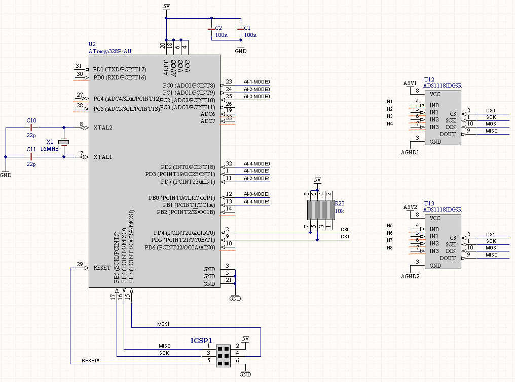
Pictures from scope:
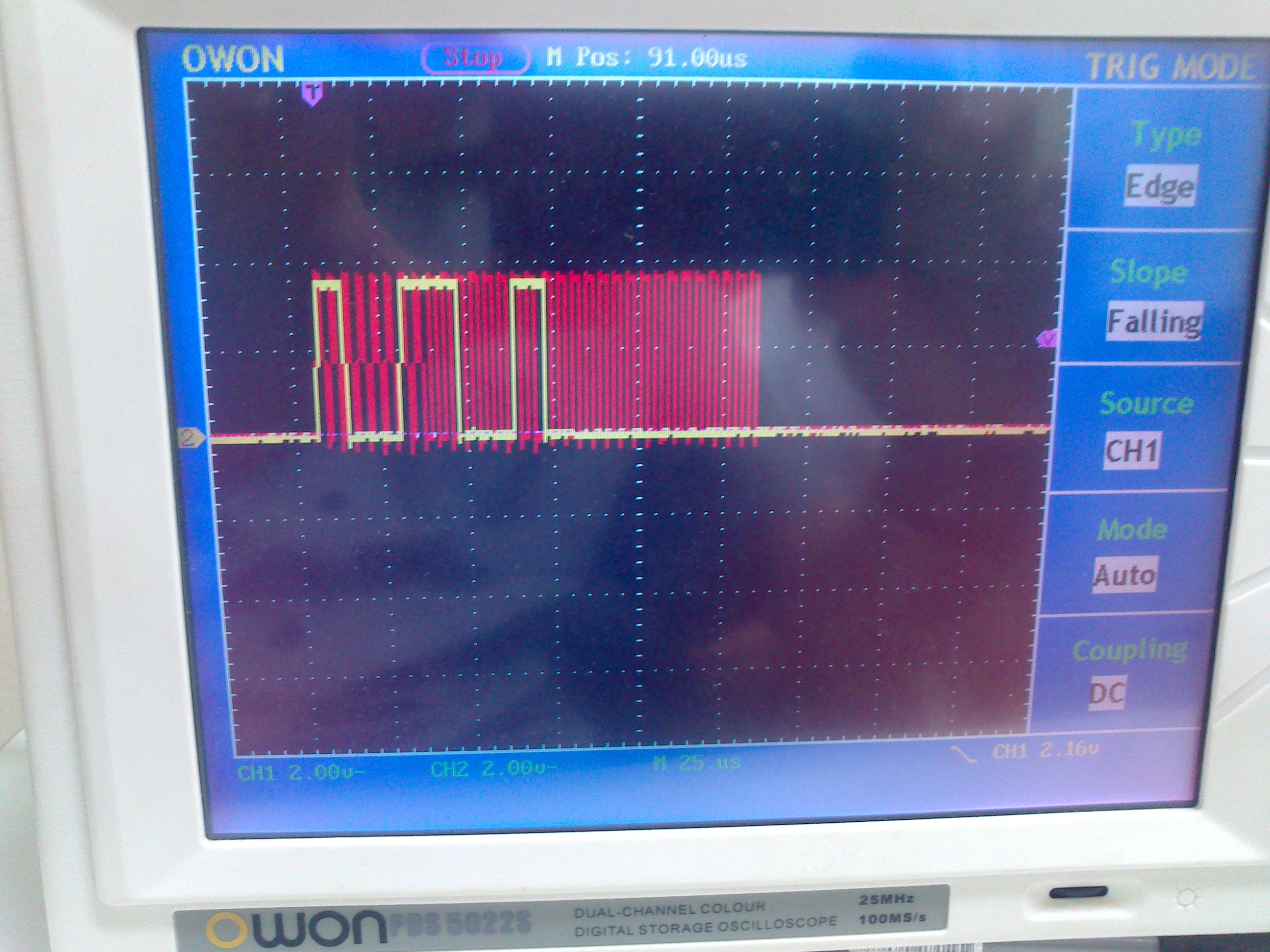
CS (Red) / SCK (Yellow)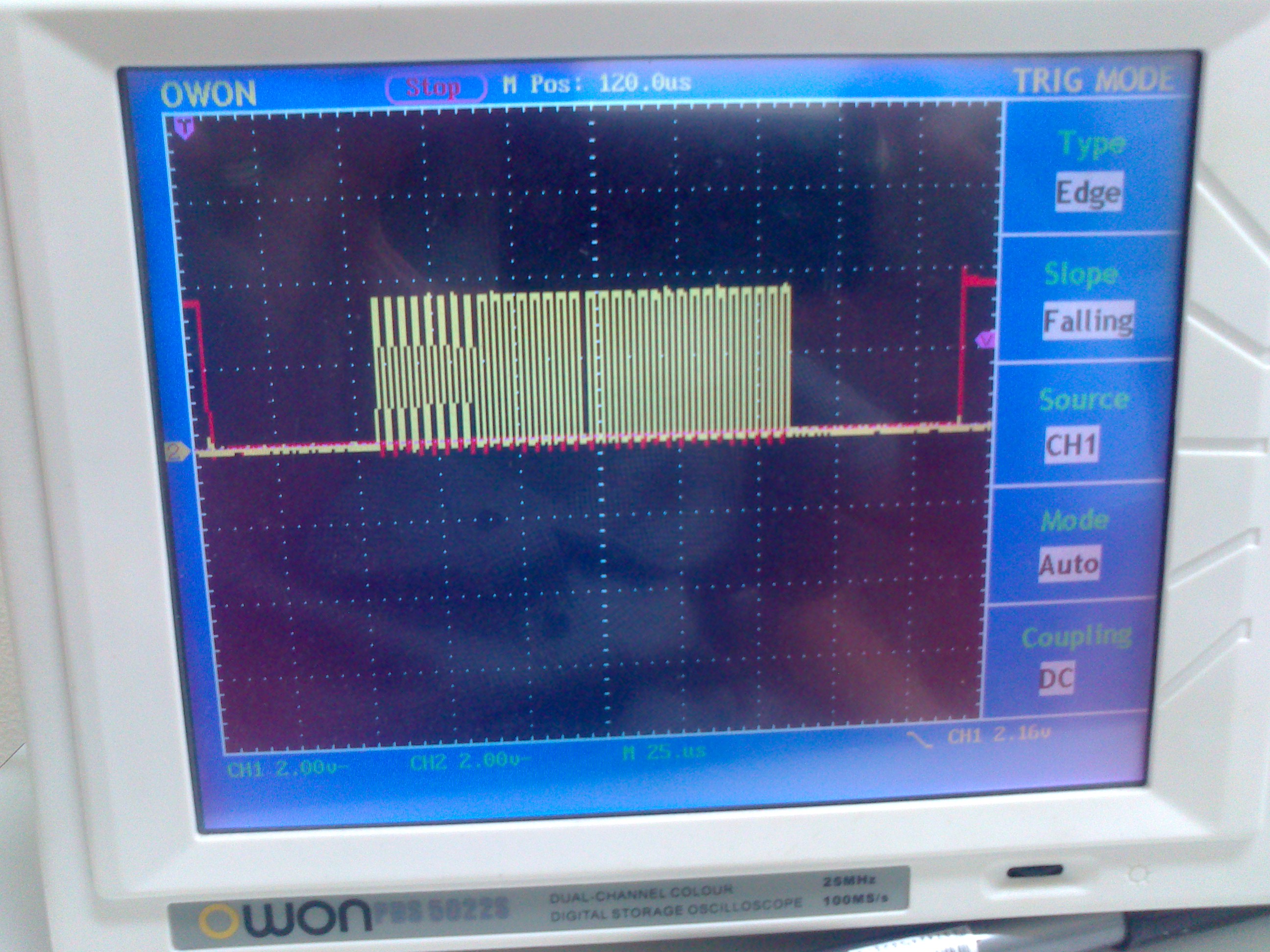
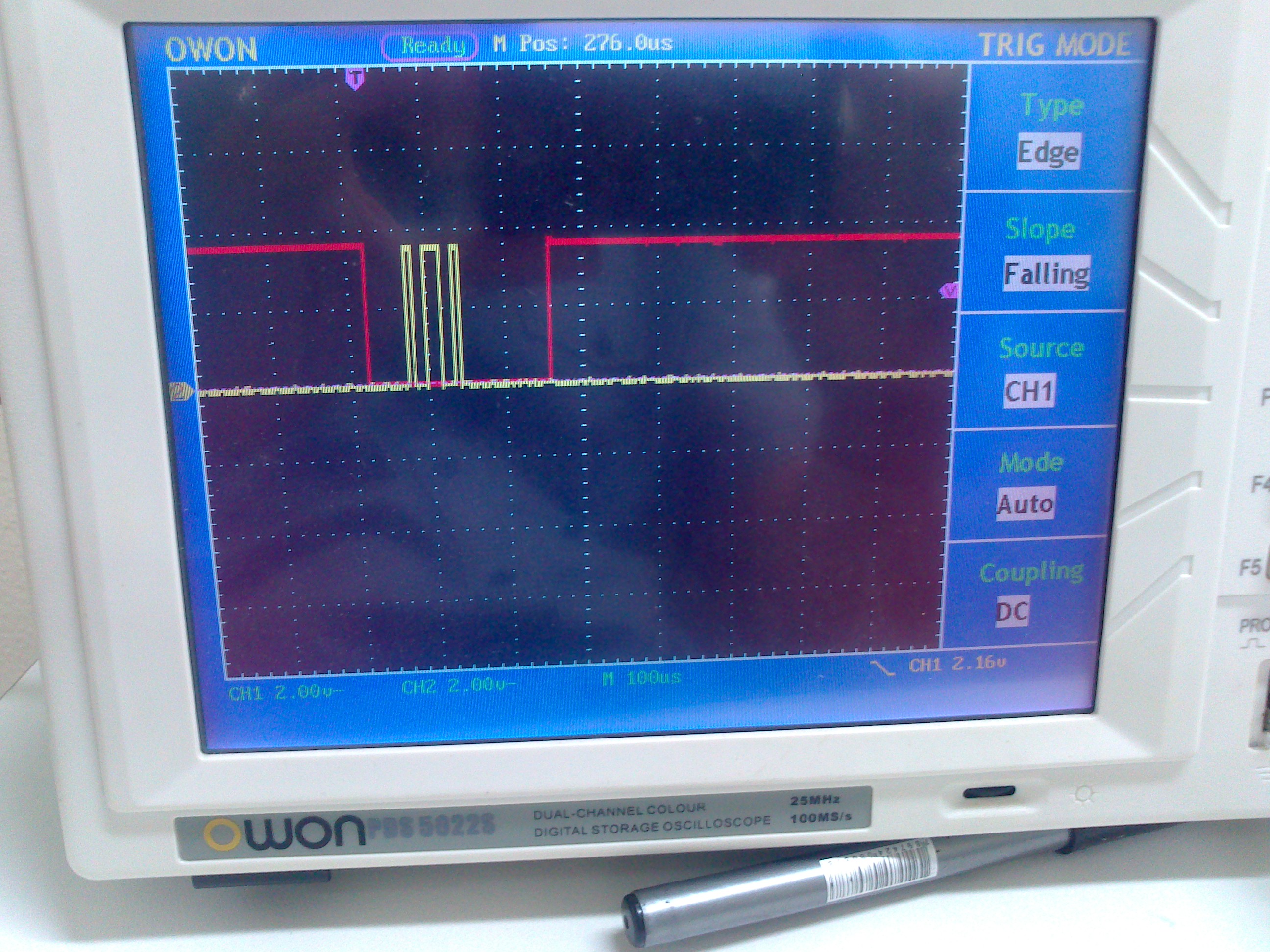
CS (Red) / MISO (Yellow)

CS (Red) / MOSI (Yellow)
SCK (Red) / MISO (Yellow)
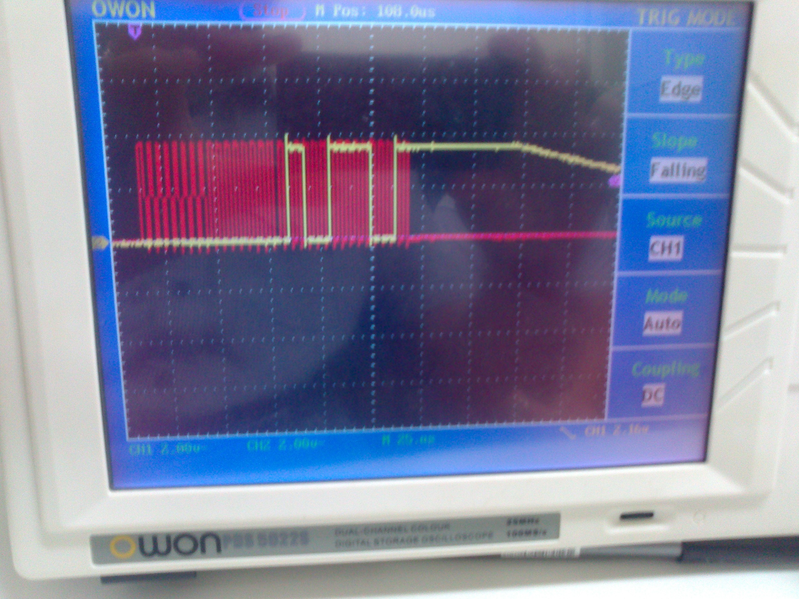
SCK (Red) / MOSI (Yellow)