This thread has been locked.

If you have a related question, please click the "Ask a related question" button in the top right corner. The newly created question will be automatically linked to this question.

ADS1672 will not do free running

Other Parts Discussed in Thread: ADS1672

Hi

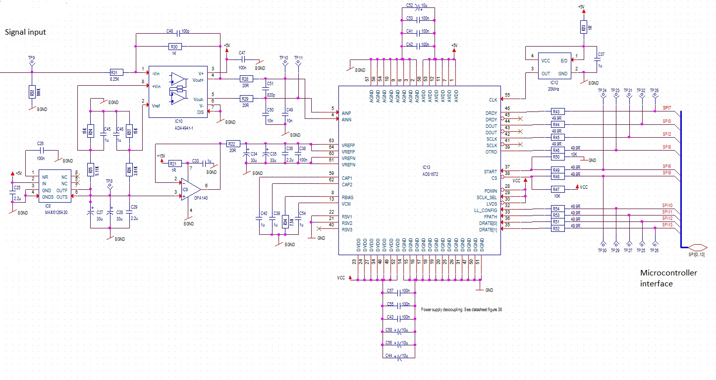
In one of our new designs, we are using the ADS1672 ADC.

When we toogle the start pin, we can get one fine ADC value, but when we hold the start pin high to make it free running, the output looks wrong.

We use an external sclk and SCLK_SEL = 1

Other setup parameters:

LL_config = 0

FPATH = 1

CS = 0

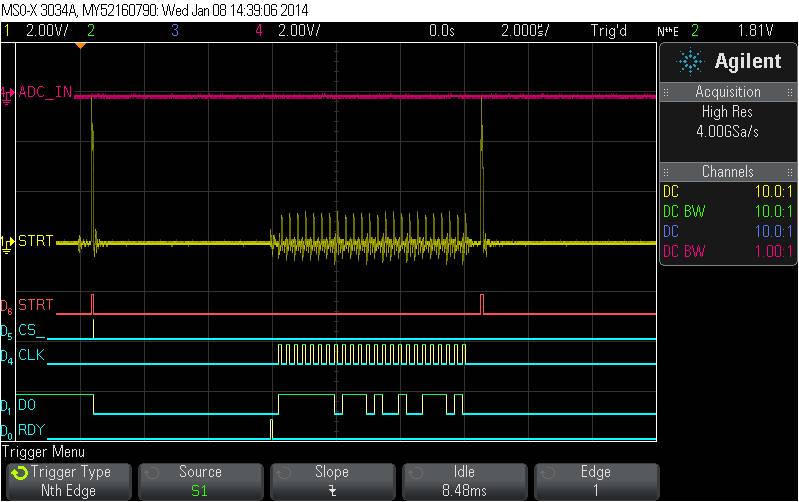
Here is an picture of a single adc measurement (start toggle) where the Dout is OK:

And here is a picture of the free running mode (start held high), where Dout is not ok:


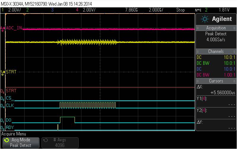
Any ideas of why we can make good measurements when toggling the start pin, but not in free running mode?

  • A couple questions:

    1.  The CLK signal shown - this is the SCLK or CLK signal?  It looks to be the SCLK, but we want to confirm

    2.  LVDS pin = ?  Assumption is that you are using CMOS compatible mode (=1)

    3.  Is the period of the DRDY pulse what you expect? (ie is the datarate correct?)

  • It is the sclk.

    lvds is set High for cmos operation

    the drdy period looks fine

  • Are you using your own board design or is this the EVM?

    What supplies are you using?  Make sure you are meeting the supply voltage for DVDD/AVDD shown in the datasheet.

  • Hi

    It is our own design which you can see below.

    BGND is the analogue ground plane and GND is the digital ground plane. They are connected just below the ADC.

    VCC is a 3.3V supply.

  • One more question:

    It there a maximum time limit for clocking out the data?

    It looks like the Data Out goes "dead" after approximately 1.7 seconds even though we only sample data at 36kSPS when the ADC is in free running mode.


  • Sorry, it should have been 1.7 microseconds and not 1.7 seconds!!!

  • There is not limit as to when you need to get the data, just so that you get it all out before the next DRDY.  At the next DRDY, the output register is updated with the new data.

    Regarding your circuit:
    There are some potential problems with the reference circuit for the device that may be causing some of the issues that you are seeing.  It looks like the capacitance on the reference it a little high.  Can't comment on specifics of what is can handle, but it seems like a lot. 
    There is also a lot of capacitance loading the reference buffer after R22 that may be causing some instability during operation.  (You can reference the buffer circuit in Figure 39 of the datasheet for an example).  You might try a quick experiment by removing the 2 large caps (C34, C35) and see if things change.

    On the analog inputs, the filters that you have could also cause some problems.  Generally, you don't want the common mode capacitors to be larger than the differential capacitor.  Any mismatch in the common mode caps could translate to voltage error that would propagate through the circuit.