This thread has been locked.

If you have a related question, please click the "Ask a related question" button in the top right corner. The newly created question will be automatically linked to this question.

DAC8832 Grounding

Other Parts Discussed in Thread: DAC8832

Hi,

I am using the DAC8832IRGY for controlling the gain of a VCA.

The VCA is powered by analog voltage (so is the DAC8832). However, the controls of the DAC8832 are from the digital domain.

Therefore, I connect the DGND to Digital_GND, AGNDF/S and PD to analog_GND. P3V3_D is digital supply, and P5V0_ANA is analog supply (see below).

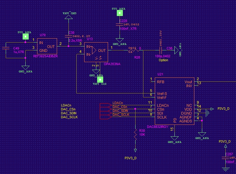
My question is weather the GND is isolated from AGNDF/S and PD as it seems that the AGND is "polluted" by noise from the digital ground. 

I would  also like to know if there is coupling between VDD and AGNDF/S or PD

Thanks,

 Avishai

  • Hi Vishay,

    DGND and AGND must be connected at some point. I don't see a connection between them from your schematic.

    Coupling between DGND and AGND may occur if the digital current loops interfere with the analog current loops. Keep the digital paths away from the critical analog paths. This can be done by physically keeping DGND and AGND away from each other. For example, connect the grounds of the supplies on the board itself, not to each other. In layout, simply keeping the digital traces away from the analog traces can reduce coupling drastically.

  • Hi, Mr. Eugenio,

    Indeed, I sent only a small portion of the schematics (only the portion tha trelates to the ADC8832)

    I also kept the connection between AGND and the DGND out of the schematics, but they are shorted through ferrite beads and an ADC.

    My question relates to the DAC chip:

    1. What is the coupling the chip between PD, AGNDF/S and GND?  Are they electrically isolated? Are they shorted? Is there resistance/capacitance between them? Can you send me the equivalent circuit between the 4 nodes (PD, AGNDF/S and GND)?

    2. I seem to have made a mistake and connect P3V3_D (3.3V, digital voltage) to the VDD input pin - instead of analog voltage. What is the coupling between VDD, and the other 4 ground nodes (PD, AGNDF/S and GND)?

    Please note that the input voltages into the VCA (that is controlled by the output voltage of this DAC) is in the range of 50uV. Noisy ground and supply of the VCA damage the input signal. I am afraid that the DAC causes leakage from the digital domain to the analog domain.


    Thanks,

     Avishai

  • Hi Avishai,

    Avishai Henley said:
    1. What is the coupling the chip between PD, AGNDF/S and GND?  Are they electrically isolated? Are they shorted? Is there resistance/capacitance between them? Can you send me the equivalent circuit between the 4 nodes (PD, AGNDF/S and GND)?

    The AGNDF/S pins are shorted internally. The thermal pad is connected to the die substrate through a thermally conductive material that is not intended to be electrically conductive. There is some small conductive property of the thermal material, though, so it is often intentionally connected to a net – typically the negative most potential of the die. In this case is AGND is connected to the thermal pad via a high impedance (megaohms). DGND and AGND are internally connected by back-to-back diodes to ensure that they are kept within 0.3V of one another. The leakage current is minimal.

    Avishai Henley said:
    2. I seem to have made a mistake and connect P3V3_D (3.3V, digital voltage) to the VDD input pin - instead of analog voltage. What is the coupling between VDD, and the other 4 ground nodes (PD, AGNDF/S and GND)?

    The coupling of any digital noise associated with the supply provided for the VDD pin is likely dominated  by other design related factors such as bulk and local decoupling capacitors or other PCB parasitics.

    Avishai Henley said:
    Please note that the input voltages into the VCA (that is controlled by the output voltage of this DAC) is in the range of 50uV. Noisy ground and supply of the VCA damage the input signal. I am afraid that the DAC causes leakage from the digital domain to the analog domain.

    The datasheet specifies a parameter called digital feed-through that describes how much of the digital signals can couple into the analog output. The digital-feed-through of this device is specified 0.2 nV-s.