This thread has been locked.

If you have a related question, please click the "Ask a related question" button in the top right corner. The newly created question will be automatically linked to this question.

ADS1281 Timing

Other Parts Discussed in Thread: ADS1281

Hello,

To implement "Read Data Continuous" in PINMODE on the ADS 1281 as shown in Figure 47 in the data sheet, I have applied the following to the listed pins;

PINMODE = HI ; MOD/DIN = LO ; PHS/MCLK = LO ; DR1/M1 = LO ; DR0/M0 = LO ;HPF/SYNC = HI;

CLK = 1MHz free running clock ; SCLK = 100KHz free running clock.

Thus CLK and SCLK are not synchronous.

In this configuration for reference, the FIR Decimation Ratio = 4096 and FIR Data Rate =62.5Hz.

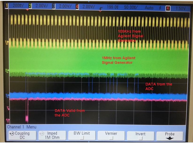
What I get (see Figure above) is a DRDY that is not synchronous with neither CLK nor SCLK, in addition the DRDY pulse width varies.

Q1. Does SCLK has to be synchronous with CLK, for DRDY to lock with either, Figure 47 implies that DRDY and SCLK are synchronous?

Q2. Why does it take the data bits so long after DRDY to appear?

Q3. I would like to run the ADS1281 in synchronous mode with an external clock applied to the RESET pin, however doing this makes DRDY stay HI.

Please direct me to a complete timing diagram for PINMODE operation with external synch.

Thank you!

AD

  • Hi AD,

    Welcome to the TI E2E Forums!

    1. It is not necessary to synchronize SCLK with CLK.
    2. The FIR filter takes 62 conversion cycles to settle. At 62.5Hz, this results in a settled conversion after ~1sec.
    3. Make sure the external clock period is an integer multiple of the data rate. Otherwise, the conversions may get continuously restarted and you'll never get a settled output.

    Pin mode is not used very often with the ADS1281 so I don't have any applications notes on the subject. I think for the most part the timing requirements will be similar to the figure on page 6 of the datasheet (ignoring DIN in pin mode).

    One thing I notice from your screenshot is that you are using a continuously running clock. I would suggest just sending SCLKs after a /DRDY pulse to clock out the data, and then stop SCLK until the next /DRDY pulse.

    Regards,
    Chris

  • Hello Chris,


    Thank you for all your answers and explanations, below are my comments and follow up questions.

    About Ans1- you answered my question, thank you!

    About Ans2- Allow me to explain you my interpretation of your answer to Q2. If an analog signal presents itself at the input at (t=0) its settled digital equivalent will present itself after the 62nd /DRDY pulse ~ 1sec later. 

    Q4.How much off is the value at the digital output at the 1st /DRDY, 2nd /DRDY..... pulse?

    About Ans3- Just to make sure, you mean the external clock that I am applying to the RESET pin. Should be 62.5Hz X N (N =1,2,3,....).

    Response to your comments;

    In our application the ADS1281 will be controlled with an FPGA in a state machine configuration, causing us to choose the PINMODE configuration for the ADS1281. 

    Q5. Regarding your screenshot comment, please explain, in PINMODE, which clock input (CLK or SCLK or /RESET) generates directly or indirectly the /DRDY output?

    Thanks again,

    AD

  • Hi AD,

    Arsham Dingizian said:

    About Ans2- Allow me to explain you my interpretation of your answer to Q2. If an analog signal presents itself at the input at (t=0) its settled digital equivalent will present itself after the 62nd /DRDY pulse ~ 1sec later. 

    Q4.How much off is the value at the digital output at the 1st /DRDY, 2nd /DRDY..... pulse?

    Correct! Regarding your additional question, I don't know the error exactly. However, you can estimate it like an RC circuit. Think of the FIR as having a time constant and after ~17-22 time constants (or 62 /DRDY periods) the filter is settled. (The 17-22 number comes from the number of RC time constants its takes an RC circuit to settle to the 24-32 bit range.)  Then you can compare the number of /DRDY pulses (or time constants) to a RC's circuit "percentage of settling" value.

    Take a look at this related forum post to see an example and a similar explanation. http://e2e.ti.com/support/data_converters/precision_data_converters/f/73/p/279012/979018.aspx#979018.

    Arsham Dingizian said:
    About Ans3- Just to make sure, you mean the external clock that I am applying to the RESET pin. Should be 62.5Hz X N (N =1,2,3,....).

    Correct!

    Arsham Dingizian said:
    Q5. Regarding your screenshot comment, please explain, in PINMODE, which clock input (CLK or SCLK or /RESET) generates directly or indirectly the /DRDY output?

    The CLK is what controls the modulator/filter. SCLK is only used to clock out the data. Therefore, /DRDY is controlled by CLK and will pulse without an applied SCLK.

    Best Regards,
    Chris

  • Hello Chris,

    Thank you for answering my questions.

    Best regards,

    AD

  • Hello Chris

    In our present application we want to use the ADS1281 it in the PINMODE,  and we are having some issues that are puzzling. We used this device in PINMODE a while back in the same circuit and it worked fine. As you know there are no timing references running the ADS1281 in the PINMODE. Our analog inputs have been checked and rechecked.

    The Digital Signals we are applying are;

    • CLK (pin1) = 2MHz free running clock (from an FPGA)
    • SCLK (pin2) = 24 synchronous (with CLK above) clocks applied to ADS1281 (from an FPGA)
    • HPF/SYNC (pin10) = Logic-HI (3.3V)
    • MOD/DIN (pin5) = Logic-Lo (0V)
    • DRDY_n(pin3) = Is generated by the ADS1281
    • MFLAG (pin11) = unused
    • DR1/M1 (pin8) = Logic-Lo (0V)
    • DR1/M0 (pin9) = Logic-Lo (0V)
    • PINMODE (pin21) = Logic-HI (3.3V)
    • PWDN_n (pin19) = Logic-HI (3.3V)
    • RESET_n (pin20) = Setup#1 Logic-HI (3.3V), except once on POR=0V

                                      = Setup#2 Externally applied negative going asynchronous clock pulses to RESET at 62.5HZ, 125Hz, 250Hz (multiples of 62.5Hz as you suggested in your response two years ago)

    As mentioned , all analog signals are present and look clean

    In Setup #1 Why, with the Analog input fixed DC the binary outputs (bit 24 to 16) randomly flip between 0 and 1?

    In Setup #2 Why DRDY doesn't activate unless my RESET rate is about 1-sec or longer?

    Thank you for your support Chris

    Arsham

  • Hi Arsham,

    Sorry for the delay. To answer your questions...

    1) It looks like you're applying a 0V differential signal, therefore you'll see output codes near zero. However, because of offset and noise you'll likely see both positive codes (close to 0x00000001 => +1) AND negative codes (close to 0xFFFFFFFF => -1). Keep in mind that the ADS1281 outputs codes in two's binary format, which the expect ion that both the most significant bit AND the least significant bit indicate the sign.

    2) If you're using continuous-sync mode then the frequency of the clock applied to RESET is very important! It must be an exact integer multiple of the data rate; otherwise, the ADC will restart the conversion - which could be preventing /DRDY from going low. Unless you need this mode, I would recommend using pulse-sync mode. I recently gave a more detailed description of when this mode may be useful (found here: e2e.ti.com/.../1916923. Keep in mind that the data rate will scale proportionally to the external clock frequency. The 250 SPS data rate assumes a nominal 4.096MHz clock. With a 2 MHz clock, your data rate will be closer to 122 SPS.

    Best Regards,
    Chris
  • Hello Chris

    Thank you for your answers, below are my follow-up questions;

    For your Answer 1:

    I am sorry for not providing the circuit diagram, to show the topology, please see circuit below, with PINMODE=1;

    The input to the ADC is provided by fully differential OPAmp with COM  input allowing DC shift to accommodate the ADC. The table following the schematics lists the voltages at the input of the ADC, The input to the Diff Amp is single ended from 0 to +5V the input to the ADC is +2.5V and +2.5V inverted


    Vin @ TP25

    Diff Amp [Volts]

    (VAIN+)-(VAIN-)

    [Volts]

    0

    -2.493

    0.500

    -1.995

    1.000

    -1.497

    1.500

    -0.999

    1.999

    -0.501

    2.499

    -0.002

    2.999

    +0.495

    3.49

    +0.993

    3.99

    +1.491

    4.49

    +1.990

    4.99

    +2.487

    Based on the table above we should have no problems with MSB 24 to 16 bits flipping.

    For your Answer 2:

    If it wasn't for table 10, stating that for PINMODE=1 only the RESET_n pin can be used as Sync input we would have used the HPF/SYNC Pin instead.

    However in paragraph PULSE-SYNC MODE does state that this mode can be used for pin or command, but never mentions RESET_n signal (pin) in Figure 38 see below: Please confirm that for PINMODE=1, you are suggesting that we apply the SYNC pulse to the HPF/SYNC (pin10) to achieve synchronization.

    I did read your post 1916923, I was somewhat concerned since we also have multiple ADCs (QTY-10 ADS1281) running from a common clock (2MHz) some of them serving two to three loops, thus having gaps could make the loop convergence problematic. I am glad you did point this out though.

    To Summarize:

    Question #1: For setup #1, I still don't understand why the MSB 24-to-16 random flipping, under what circumstances could this happen?

    A possible hint, while adjusting (up or down within the 0 to +5V scale) the DC input voltage, we noticed that during the voltage transition the MSBs would be very stable while the LSBs appeared as if they were counting up, once we stop changing the DC level (within ~1sec) the MSBs and LSBs would go back to random flipping.

    Question #2: (Just a statement)  For setup #2, please confirm that for PINMODE=1, you are suggesting to have POR on the RESET_n (pin 20), and apply a SYNC clock to on the HPF/SYNC (PIN10).

    Question #3: For setup #2, with exactly 2.000MHz, with FIR decimation of 4096 (FIR data rate of 122.07 SPS) what should the RESET_n Pulse Width and Period be? How does this relate (or fold into) to the 62.5Hz multiples for the RESET_n.

    Regards,

    Arsham

  • Hi Arsham,

    Sorry, It's been awhile since I've looked at the pinmode on this device. In pinmode, there is actually no option for continuous-sync mode, you can only use pulse convert mode, as shown in table 9:

    NOTE: With pinmode = 1 and MOD = 0, the HPF/SYNC pin controls the high-pass filter and the nRESET pin is used for synchronizing conversions.

    1. Have you looked into the possibility of an SPI communication issue? The ADS1281 data should be read on the rising edge of SCLK (SPI mode 0). Otherwise, I'm not sure why you would see the MSBs flip. LSBs flipping is normal due to noise
    2. Do not apply a clock to the SYNC pin while in pinmode - The nRESET pin controls synchronizations in pinmode. Is there a reason why you need to re-synchronize the ADC so often?
    3. I would go by the SYNC pin timing as shown in figure 38 and table 11 for synchronizing the ADC (using pulse-sync mode).

    Best Regards,
    Chris

  • Hello Chris,

    No problem

    I appreciate your help.

    By the way we discovered that the HPF/SYNC pin was pulled HI during previous testing and we forgot about it, causing the blocking of the DC signal. Things are working fine now an we will use the SYNC timing.

    Best Regards,

    Arsham