This thread has been locked.

If you have a related question, please click the "Ask a related question" button in the top right corner. The newly created question will be automatically linked to this question.

DAC7716 problem

Other Parts Discussed in Thread: TMS320F28335, DAC7716EVM, DAC7716

Hello,

I am using the DAC7716EVM and DSP TMS320f28335 for converting DAC by SPI communication. I tried to setup and gave the simple code to the DSP. 

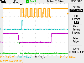
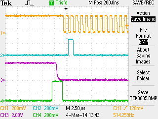
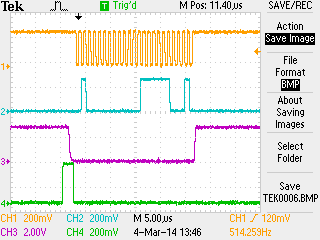
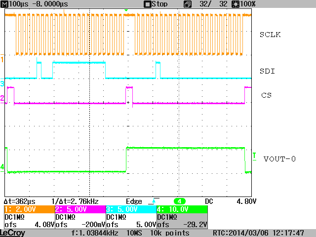
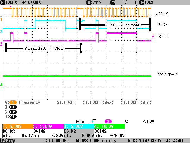
The signal from DSP is correct (I see on the oscilloscope), but the output of the DAC is seemly not working (I gave the analog input is +-11V, ref is 5V, digital input is 3.3V).

Can anyone help me to check my code or if someone have the sample code to show me the correct way to communicate this EVM board. Many thanks!!!!

Here my code:

#include "DSP2833x_Device.h"     // DSP2833x Headerfile Include File   
#include "DSP2833x_Examples.h"   // DSP2833x Examples Include File   
   
 
void delay_loop(void);   
void spi_fifo_init(void);   
void InitGpio(void);   

void tx_data_dac(Uint16,Uint16);
Uint16 shift_4_bits (Uint16);
void CS(int);
void chanel_0(Uint16,Uint16);
void LDAC(int);
void Reset_DAC(int);


interrupt void spia_txisr(void);
interrupt void spia_rxisr(void);

extern void InitPieCtrl(void);
extern void InitPieVectTable(void);  
int counter=0;
int i[8];
int count=0;
Uint16 j= 1024;
void main(void)   
{   


   InitSysCtrl();   

//   InitSpiaGpio();
    InitGpio();  
   
// Step 3. Initialize PIE vector table:   
// Disable and clear all CPU interrupts   
   DINT;   
   IER = 0x0000;   
   IFR = 0x0000;   
   
    InitPieCtrl();
    InitPieVectTable();

    EALLOW;
    PieVectTable.SPITXINTA=&spia_txisr;
    PieVectTable.SPIRXINTA=&spia_rxisr;
    EDIS;


    PieCtrlRegs.PIECTRL.bit.ENPIE = 1;  // Enable the PIE block
    PieCtrlRegs.PIEIER6.bit.INTx2 = 1;    // TXSPI interrupt
    PieCtrlRegs.PIEIER6.bit.INTx1 = 1;    // RXSPI interrupt
    IER=0x20;    // int6 enable


    EINT;
    ERTM;
    
// Initialize the SPI only
    spi_fifo_init();     
// Reset DAC by hardware
    Reset_DAC(1);
    Reset_DAC(0);
//Latch is not transparent
    LDAC(0);
// Loop for transer SPI
   while(1) {
   if (count==2)
       {
    //    CS(1);
         LDAC(1);     // open latch to send out voltage
        SpiaRegs.SPIFFTX.bit.TXFFIENA    = 0;
        count = 0;
        delay_loop();    // wait a bit before next transmitting
    //    delay_loop();
        LDAC(0); // close latch to wait for next digital input
    //    CS(0);
        SpiaRegs.SPIFFTX.bit.TXFFIENA    = 1;

    
     }
   
   }
       
}   
   
   
// Some Useful local functions   
void delay_loop()   
{   
    long      i,j;   
    for (i = 0; i < 500000; i++) {
    //    for (j = 0; j < 10; j++) {}
    }  
     
}   
   
void spi_fifo_init()   
{   
// Initialize SPI FIFO registers   
 
    SpiaRegs.SPICCR.bit.SPISWRESET  = 0;       // reset SPI - 0x000F
    SpiaRegs.SPICCR.bit.SPILBK      = 1;       //  loop back
    SpiaRegs.SPICCR.bit.CLKPOLARITY = 1;       // clk polarity is falling edge
       SpiaRegs.SPICCR.bit.SPICHAR     = 11;     // data length = 12b (0-->15 means 1 bit to 16bits)

    SpiaRegs.SPICTL.bit.OVERRUNINTENA = 0;     // disable rx overrun flag bit interrupts (SPISTS.7)
       SpiaRegs.SPICTL.bit.CLK_PHASE     = 0;     // Enable normal phase - 0x0002
       SpiaRegs.SPICTL.bit.MASTER_SLAVE  = 1;     // master mode
       SpiaRegs.SPICTL.bit.TALK          = 1;     // enable talk
       SpiaRegs.SPICTL.bit.SPIINTENA     = 1;     // SPI int disable
 
    SpiaRegs.SPIFFTX.bit.SPIFFENA    = 1;        // FIFO transmit enable
    SpiaRegs.SPIFFTX.bit.TXFIFO        = 1;        // re_enable FIFO transmit enable
//    SpiaRegs.SPIFFTX.bit.TXFFST        = 0xFFFFF;        //
    SpiaRegs.SPIFFTX.bit.TXFFIENA    = 1;        // FIFO transmit interrupt
//    SpiaRegs.SPIFFTX.bit.TXFFIL        = 0x02;
//    SpiaRegs.SPIFFTX.bit.TXFFINTCLR = 1;       // clr TXFFINT flag in SPIFFTX


    //SpiaRegs.SPIFFRX.bit.RXFIFO        = 1;        // re_enable FIFO receive enable
    SpiaRegs.SPIFFRX.bit.RXFFIENA    = 1;        // FIFO receive interrupt
//    SpiaRegs.SPIFFRX.bit.RXFIFORESET= 1;

//    SpiaRegs.SPIFFCT.all = 200;                    // delayed transfer
    //       SpiaRegs.SPISTS.all=0x0000;   
       SpiaRegs.SPIBRR= 36;           // Baud rate with freq 1Mhz  
    
  // SpiaRegs.SPIPRI.all=0x0010;   
   
   SpiaRegs.SPICCR.bit.SPISWRESET=1;  // Enable SPI   
   
}   
   
void InitGpio()
{

   EALLOW;
/* Enable internal pull-up for the selected pins */
// Pull-ups can be enabled or disabled by the user.  
// This will enable the pullups for the specified pins.
// Comment out other unwanted lines.

    GpioCtrlRegs.GPAPUD.bit.GPIO16 = 0;   // Enable pull-up on GPIO16 (SPISIMOA)
    GpioCtrlRegs.GPAPUD.bit.GPIO17 = 0;   // Enable pull-up on GPIO17 (SPISOMIA)
    GpioCtrlRegs.GPAPUD.bit.GPIO18 = 0;   // Enable pull-up on GPIO18 (SPICLKA)
    GpioCtrlRegs.GPAPUD.bit.GPIO19 = 0;   // Enable pull-up on GPIO19 (SPISTEA)


//    GpioCtrlRegs.GPBPUD.bit.GPIO54 = 0;   // Enable pull-up on GPIO54 (SPISIMOA)
//    GpioCtrlRegs.GPBPUD.bit.GPIO55 = 0;   // Enable pull-up on GPIO55 (SPISOMIA)
//    GpioCtrlRegs.GPBPUD.bit.GPIO56 = 0;   // Enable pull-up on GPIO56 (SPICLKA)
//    GpioCtrlRegs.GPBPUD.bit.GPIO57 = 0;   // Enable pull-up on GPIO57 (SPISTEA)

/* Set qualification for selected pins to asynch only */
// This will select asynch (no qualification) for the selected pins.
// Comment out other unwanted lines.

    GpioCtrlRegs.GPAQSEL2.bit.GPIO16 = 3; // Asynch input GPIO16 (SPISIMOA)
    GpioCtrlRegs.GPAQSEL2.bit.GPIO17 = 3; // Asynch input GPIO17 (SPISOMIA)
    GpioCtrlRegs.GPAQSEL2.bit.GPIO18 = 3; // Asynch input GPIO18 (SPICLKA)
    GpioCtrlRegs.GPAQSEL2.bit.GPIO19 = 3; // Asynch input GPIO19 (SPISTEA)
 
//    GpioCtrlRegs.GPBQSEL2.bit.GPIO54 = 3; // Asynch input GPIO16 (SPISIMOA)
//    GpioCtrlRegs.GPBQSEL2.bit.GPIO55 = 3; // Asynch input GPIO17 (SPISOMIA)
//    GpioCtrlRegs.GPBQSEL2.bit.GPIO56 = 3; // Asynch input GPIO18 (SPICLKA)
//    GpioCtrlRegs.GPBQSEL2.bit.GPIO57 = 3; // Asynch input GPIO19 (SPISTEA)

    
/* Configure SPI-A pins using GPIO regs*/
// This specifies which of the possible GPIO pins will be SPI functional pins.
// Comment out other unwanted lines.

     GpioCtrlRegs.GPAMUX1.bit.GPIO0 = 0; // Configure pins as GPIO
    GpioCtrlRegs.GPAMUX1.bit.GPIO2 = 0;
    GpioCtrlRegs.GPAMUX2.bit.GPIO22 = 0;
    GpioCtrlRegs.GPAMUX1.bit.GPIO12 = 0;
    GpioCtrlRegs.GPAMUX2.bit.GPIO26 = 0;
    GpioCtrlRegs.GPAMUX2.bit.GPIO27 = 0;

    GpioCtrlRegs.GPADIR.bit.GPIO0 = 1; // output
    GpioCtrlRegs.GPADIR.bit.GPIO2 = 1; // control Uni-Bip B
    GpioCtrlRegs.GPADIR.bit.GPIO22 = 1; // control Uni-Bip A
    GpioCtrlRegs.GPADIR.bit.GPIO12 = 1; // control LDAC pin 17
    GpioCtrlRegs.GPADIR.bit.GPIO26 = 1; // control CS pin
    GpioCtrlRegs.GPADIR.bit.GPIO27 = 1; // control Reset DAC RST

    GpioDataRegs.GPACLEAR.bit.GPIO2 = 1; // control Uni-Bip B - clear bit means Bipolar +-
    GpioDataRegs.GPACLEAR.bit.GPIO22 = 1; // control Uni-Bip A - clear bit means Bipolar +-
    GpioDataRegs.GPACLEAR.bit.GPIO12 = 1; // control LDAC - transparent latch
    GpioDataRegs.GPASET.bit.GPIO26 = 1; //  CS pin active low
    GpioDataRegs.GPACLEAR.bit.GPIO27 = 1; //  Reset - active low
    GpioDataRegs.GPASET.bit.GPIO27 = 1; // Not Reset - active low


    GpioCtrlRegs.GPAMUX2.bit.GPIO16 = 1; // Configure GPIO16 as SPISIMOA
    GpioCtrlRegs.GPAMUX2.bit.GPIO17 = 1; // Configure GPIO17 as SPISOMIA
    GpioCtrlRegs.GPAMUX2.bit.GPIO18 = 1; // Configure GPIO18 as SPICLKA
    GpioCtrlRegs.GPAMUX2.bit.GPIO19 = 1; // Configure GPIO19 as SPISTEA

    EDIS;
}
interrupt void spia_txisr(void)
{

    count++;
/*    if(j<=1280)    {j++;}
    else
    {j=1024;}
    chanel_0(j,0); */
     //tx_data_dac(0,j);
    chanel_0(1200,1100);
    SpiaRegs.SPIFFTX.bit.TXFFINTCLR=1;
    PieCtrlRegs.PIEACK.all |= 0x20; //  Group 6
}

interrupt void spia_rxisr(void)
{    
     SpiaRegs.SPIFFRX.bit.RXFFOVFCLR=1;
    SpiaRegs.SPIFFRX.bit.RXFFINTCLR=1;
    PieCtrlRegs.PIEACK.all |= 0x20; //  Group 6
}


void tx_data_dac(Uint16 first_half,Uint16 second_half)
{
    switch(count)
    {
         case 1: {SpiaRegs.SPITXBUF = shift_4_bits(first_half); break;}
        case 2: {SpiaRegs.SPITXBUF = shift_4_bits(second_half); break;}
    }
}

Uint16 shift_4_bits (Uint16 data)
{
    data = data<<4;
    return data;
}
void chanel_0(Uint16 first_half,Uint16 second_half)
{
    if (first_half<1024) {first_half=1024;}
    if (first_half>1279) {first_half=1279;}
//    first_half = 1024 + first_half;

//    if (second_half <256) {second_half=256;}
//    if (second_half >3840) {second_half=3840;}
    tx_data_dac(first_half,second_half);
}
void CS(int state)
{
    if (state|=0)
    {
        GpioDataRegs.GPACLEAR.bit.GPIO26 = 1; // begin to transmit
    }
    else
    {
        GpioDataRegs.GPASET.bit.GPIO26 = 1; // stop to transmit
    }
}


void Reset_DAC(int state)
{
    if (state|=0)
    {
        GpioDataRegs.GPACLEAR.bit.GPIO27 = 1; // 1 is Reset
    }
    else
    {
        GpioDataRegs.GPASET.bit.GPIO27 = 1; // 0 is Run
    }
}
void LDAC(int state)
{
    if (state|=0)
    {
        GpioDataRegs.GPACLEAR.bit.GPIO12 = 1; // LDAC transparent
    }
    else
    {
        GpioDataRegs.GPASET.bit.GPIO12 = 1; //
    }

  • Hi Duy,

    Thank you for all the information. First of all I will need to take a look at some scope captures of your digital inputs. A schematic diagram will help me debug the circuit as well.

    Regards,

  • Hi Eugenio,

    Thanks for your reply

    Here my fig about my SPI input. First I want to set channel 0 (4 first bit address: 0100) and value to be 0x000 (12bit data). I send 2 packages of 12bits continuously for the required frame of 24bits as instruction in datasheet of DAC7716.

    The 2nd signal is connected to SDI pin of DAC 

    The 3rd signal is connected to CS pin

    The 4th is connected to LDAC to make tha latch transparent when the clock begin.

    Other register I have not set any value, let it as default from reset...(gain at 4)

    Some bigger pictures:

    I even change the value of data but the output voltage give the nonsense value (the same for all 4 output channel but I just assign the address for the 1st channel):

    Could you please check and give me advice!!!!

    Thanks

    Duy

  • Duy,

    From the scope captures it seems that you are writing data on the rising edges of SCLK. The DAC7716 uses the falling edge of SCLK to latch in the data. Shifting your data by half an SCLK cycle should make it work.

    As a side note. If you are planning on using it as a transparent, you can just tie LDAC LOW and the DAC output will update on the 24th falling edge of SCLK. There is not need to pulse LDAC before the frame.

    Let me know if this solves your issue.

  • Hi Eugenio,

    I have changed like your suggestion, but the result is still nothing new.

    I am thinking whether I set up the circuit correct or not (supply voltage, ref voltage...) But I have followed the datasheet and nothing happened.

    Do you have any reference material about this EVM or sample code about this???

    Thanks

  • The next step would be to review your schematic in order to make sure that everything is connected correctly. Can you share a snapshot of your schematic? I need to see what values you are supplying to the EVM. If you can just describe what/where you are supplying power/signals to the EVM, that would be sufficient.

    Huynh Anh Duy Nguyen said:
    Do you have any reference material about this EVM or sample code about this???

    Unfortunately there is no sample code for this. As far as reference material for the EVM, there is not additional documentation for the EVM but I can get back to you with some scope captures from the EVM.

  • Hello Eugenio,

    Thank for your reply,

    It is very hard to see my schematic because I am taking the experiment with very basic components, so I will describe which pins connected each other:

    1) I have 1 DSP board for general purpose TMS320F2885 and the DAC7716EVM.

    2) I used the SPI channel A of the DSP (only 3 pins: CLK, CS and MOSI) which connect directly with CLK, CS and SDI pins of DAC7716.

    3) For the supply input of DSP from the adapter which provide 3.3V for normal operation

    4) Supply voltage for DAC7716: AVDD = +11v; AVSS = -11V; Digital Voltage = 3.3V. Both 2 boards are connected the same GND.

    5) For set up the board, I just let it as default (gain = 4, Ref Voltage from the 5v or 2.5v on board), both channel A & B are set to Bipolar (set switch S1 to 0 for both channel).

    Then I give the SPI input which I have mentioned above, but the out put is just nonsense. (usually the Vout 0 and Vout 1 are equal and approximately 0.28V)

    One thing is when I measure the ref voltage when set the switch S2 and S3 at 5V, the real voltage is just about 4.7V. Is this ok or not???

    Those all what I have done until now.

    Best regards!!! 

    Duy

  • I just noticed that your digital signals are heavily attenuated. They are about 300mV in amplitude. A minimum voltage of 2.1V is required by the device in order to register a HIGH signal.

    Check to see if you can correct this. 

  • Hi,

    I measured the output signal at High is about 3.24V, I think this enough to get high or low level.

  • Duy,

    I did not notice this earlier but the sequence is not correct. Refer to page 16 in the DAC7716 datasheet for the frame structure.

    The correct code should be 0000 0100 [12BITDATA] 0000.

    I implemented this in the lab for reference. As you can see below. 

    I should have noticed this sooner. Let me know if there is anything else you need.

  • Hi,

    You are right, I gave the wrong frame for the SPI input. One thing I missed is the +5VD to supply for the chip 7716. However, when I applied the same input like you, the output still keep 0V (although I tried many other values for data)

    I think now my SPI input is correct thank to your information. The board seemly does not work with any input.

    I captured some pictures and give the marks of what I have supplied to the DAC board, Could you please take a look, maybe I have missed anything:

    1) The input pins (J2A) and switch S1:

    2) The supply voltages:

    3) The output and Ref voltage:

    PS: I have some doubt that:

    1) How can we know the shift register get the sequence of pulse correctly??? How can we debug this issue???

    2) When I give the supply to the input SDI, I observed the SDO pin on oscilloscope, the pulse is similar but lag 1 or 2 bits (means SDI: 0000 0100 0111 1111 1111 0000 ->> SDO: 0000 0010 0011 1111 1111 1000)? Is it normal???

    3) In page 22 of datasheet, the Power-Supply Sequencing; is it important for a simple conversion???

    4) Do we need to set up anything about Zero or Gain calibration???

    Thank in advanced!!!!

    Duy

  • Duy,

    Huynh Anh Duy Nguyen said:
    1) The input pins (J2A) and switch S1:

    If you want to control LDAC through LDAC2 you must switch JP1 to position 1-2. Currently it is being controlled by LDAC1.

    If you want LDAC to be grounded at all times, allowing for transparent DAC updates, S1.1 must be a 1. This will connect LDAC to GND.

    S1.2 is UNI/BIPB.

    S1.3 is /RST, which is currently HIGH. Allowing the device to operate normally.

    S1.4 is UNI/BIPA.

    Huynh Anh Duy Nguyen said:
    1) How can we know the shift register get the sequence of pulse correctly??? How can we debug this issue???

    You can readback the DAC registers as explained in page 24 of the DA7816 datasheet.

    The readback command is 1000 ADDR XXXX XXXX XXXX XXXX XXXX XXXX XXXX XXXX

    For VOUT-0 ADDR = 0100

    I took a plot for your reference.

    Huynh Anh Duy Nguyen said:
    2) When I give the supply to the input SDI, I observed the SDO pin on oscilloscope, the pulse is similar but lag 1 or 2 bits (means SDI: 0000 0100 0111 1111 1111 0000 ->> SDO: 0000 0010 0011 1111 1111 1000)? Is it normal???

    No, I don't think this shift is normal. As you can see on the plot above, SDO updates during the rising edge of SCLK and is valid during the falling edge of SCLK. A plot of this behavior may help me figure out what is going on.

    Huynh Anh Duy Nguyen said:
    3) In page 22 of datasheet, the Power-Supply Sequencing; is it important for a simple conversion???

    Yes, this sequencing is important to the start-up of the device. The device may latch the wrong values at start-up if the sequence is not used. Keep in mind that there are product variations. Some devices may miss-behave while others might not.

    Huynh Anh Duy Nguyen said:
    4) Do we need to set up anything about Zero or Gain calibration???

    The zero and gain calibration are optional. The zero and gain calibrations are in place in order to reduce the offset and gain errors that change from one device to another. The maximum offset and gain errors before user calibration are specified to be ±0.5LSB. If you wanted to calibrate the device to an even smaller error, you would have to measure the offset and gain errors of each device and program the device's registers accordingly. The easiest way to do this is using a two point line. Take two points, (usually from 1/4 and 3/4 of full scale) and find the equation of the line( y = m*x+b) m being the slope (gain) and b being the offset.

    If you need me to expand more on any of my answers, please feel free to ask.

  • Hi,

    Ok, your comments are really helpful to me.  I have checked again the pins on the board by the VOM. It is very surprised that some switches or pins are not placed as in the User guide of DAC7716 mentioned. 

    Then I have placed the right pins for right function and the outputs are functioning correctly and accurately now.

    Thanks again, if I have any further questions,, I will post here!!!

    DUY

  • Eugenio Mejia said:

    Yes, this sequencing is important to the start-up of the device. The device may latch the wrong values at start-up if the sequence is not used. Keep in mind that there are product variations. Some devices may miss-behave while others might not.

    So if I don't use power sequencyng and just reset the DAC with RST pin some time after power up I sholud be ok?

  • Hi Matjaz,


    Matjaz Tome said:
    So if I don't use power sequencyng and just reset the DAC with RST pin some time after power up I sholud be ok?

    This depends on the device. I do not know the answer for the DAC7716. The datasheet does not mention this specifically so I had to forward this question to the digital designers of the device. I am awaiting an answer from them.

    I will let you know their answer as soon as I get it.