This thread has been locked.

If you have a related question, please click the "Ask a related question" button in the top right corner. The newly created question will be automatically linked to this question.

TSW1200EVM with a ADS42B49EVM

Other Parts Discussed in Thread: ADS42B49EVM, ADS42B49, ADS62P49

Hi,

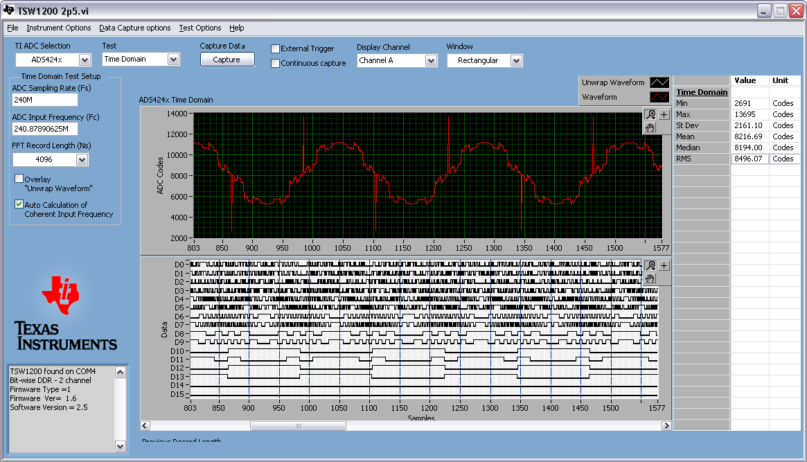
I'm trying to use the TSW1200EVM  Rev C with a ADS42B49EVM.  I have the ADS424X option selected in the GUI, but my captured signals does not look correct.  Is this the correct option to use?  Is this board (ADS42B49EVM) not supported by the TSW1200EVM firmware.

  • Daniel,

    This request came from the data converter apps team.

    "I think the digital interfaces between the two devices are identical. Can you describe some of the symptoms? Any capture possible (with distorted data – can you get a screen shot?) or no capture at all?"

    Can you post some screen captures?

    I am also working on an alternative.

    Aaron 


  • Hi,

    As Ken C pointed out offline, the TSW1400 is the newer more full featured replacement for the TSW1200, complete with a brand new GUI that installs on Windows 7, etc.

    But - the TSW1200 does support the ADS42B49 EVM.  I see no reason why it would not.   The data format of the sample data across the Samtec connector is just like the ADS62P49 family.  But there can be  minor differences sometimes.  I seem to remember that the LVDS data for the P49 family was inverted through the connector and we had to invert it back with the FPGA firmware.   It is possible that the ADS42B49 EVM might not have such an inversion.  We have in the past instructed the layout person to route the LVDS straight to the connector without concern for inversion as we could always fix it in the FPGA.  That is about the only thing that can go wrong between the two different types of EVMs.   But - I just looked at the TSW1200 ini files for the two EVMs and they are identical for the description of the sample data into the TSW1200 so we seemed to think the two EVMs look the same to the TSW1200 when we released the EVMs.  No evidence of LVDS inversion, that is.

    An example of the 'bad' capture would help.  Also, what revision of the TSW1200 GUI are they using?   What revision of the firmware does the TSW200 GUI report when it initializes?  (like firmware version 1.6 for example.)

    (And one final plug for the TSW1400 as the best fix for the issue in the long run.)

    Regards,

    Richard P.

  • Richard/Aaron,

    Here are two captures of a 241MHz signal at 3dBm and 5dBm.  Something wrong appears to happen around the zero crossing of the signal (.. maybe inverted data?) and if I increase the amplitude to 5dBm, the signal gets even more distorted.

  • Hi - I'm working with Dan on the ADS42B49 eval....we did get the TSW1200 to work properly by setting

    Clock line Skew = 20.

    It had been 0 in the original file.  We did get a TSW1400 as well which is having some different problems - but I'll start a new thread for that.


    Thanks - Eric

  • Hi,

    Hmmm. I'm glad you got it to work, but I have not had to do that with the ini file.   In case it helps shed any light on what that ini file setting means, attached is a sketch of how the ADC interface into the FPGA is implemented.  The Xilinx IDELAY cells are present on every LVDS input pair, and the IDELAY is essentially a tapped delay line with each delay increment equal to about 75ps.  The ini file for the EVM lets you set an IDELAY tap setting for the clock and another IDELAY tap setting for all of the data pairs.   Maybe adding enough skew to the clock is similar to inverting the clock.   Did you leave data line skew set to 10?   There is another ini file entry called Clock Edge, and if it is really that the clock is inverted somewhere in the path then setting this entry to =1 might be the better solution.   Delaying the clock might mean you need a different skew setting for slower sample rates due to longer clock period.  But if it works for what you are doing, maybe we don't want to monkey with it.

    And yes, if you do start a separate posting with any issues you might be having with the TSW1400 then we will address those at that time.

    Regards,

    Richard P.

  • Ok - based on your comments, I think we modified more than just the Data line skew...I've copied in the timing portion of the file for reference.

    Max sample Rate=250E6

    Data format=Offset Binary

    Output format=Bit-wise DDR - 2 channel

    Clock Edge=0

    Data line skew=0

    Clock line Skew=20

    Hardware bit offset=0