This thread has been locked.

If you have a related question, please click the "Ask a related question" button in the top right corner. The newly created question will be automatically linked to this question.

DAC 8734EVM powering UP/initialization

Other Parts Discussed in Thread: DAC8734, DAC8734EVM

Hi,

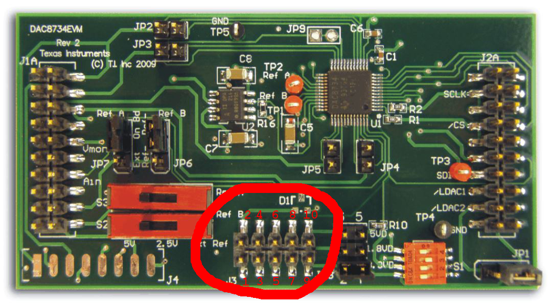
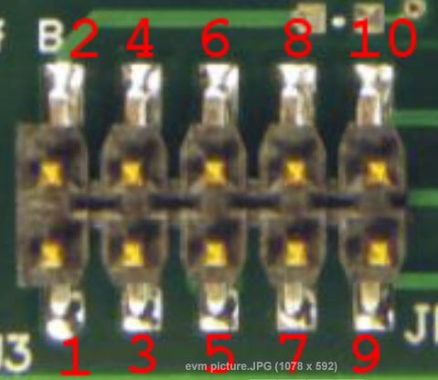
I just bought DAC8734 board.Can anyone tell me the powerup sequence pins in EVM.

Which pins does the following signals denote.

DVdd-

IOVdd-

AVss-

AVdd-

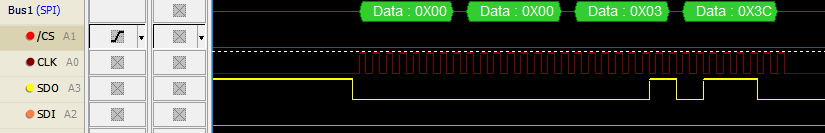
I know this is the sequence for powerup from the datasheet, but couldn.t map the signlas on the EVM.

your help is very much appreciated.

Thanks,

Anbu

  • Hello Anbu,

    I would be glad to assist you with this issue.

    I know you mentioned that you knew the power-up sequence from the DAC8734 datasheet. I just want to paste it here for someone else's reference if they see this post.

    Anbazhagan Sakthivel said:
    Can anyone tell me the powerup sequence pins in EVM.

    The power-up sequence for the DAC8734 can be found on page 22 of the datasheet.

    To break it down from first to last:

    1. DVDD, IOVDD & UNI/BIP-x (In any order, or all together.)
    2. AVSS
    3. AVDD (Can be ramped at the same time as AVSS, but NOT before.)
    4. REF-x

    Anbazhagan Sakthivel said:
    Which pins does the following signals denote.

    If you are using the MMB0 motherboard, most of the voltages are supplied to the EVM, except AVDD and AVSS. Remember to remove J13A from the MMB0. Otherwise it will supply +5V to AVDD.

    This means that DVDD, IOVDD & UNI/BIP-x will be supplied at the same time.

    You have to then power up AVSS and AVDD according to the power-up sequence instructions above.

    The on-board REF-x are dependent on AVDD, so REF-x will always power-up after AVDD. If you are applying external REF-x, then you have to make sure that they power up AFTER AVDD.

    The EVM power sequence with the MMB0 will be:

    1. Power-up MMB0
    2. Apply AVSS
    3. Then AVDD (or at the same time as AVSS.)
    4. Finally apply REF-x if using external reference. (On-board reference will always power-on after AVDD.)

    As stated above, if you are using the MMB0 you only have to externally supply AVDD & AVSS (External REF-x is optional). I will describe all the power inputs in case you want to use the MMB0 without the MMB0.

    Most of these power inputs are on the power block (J3) on the bottom center of the DAC8734EVM. 

    • AVDD = J3[1] =+VA
    • AVSS = J3[2] = -VA
    • DVDD = J3[10] = +5VD
    • IOVDD has a jumper that allows you to select the voltage. The options are selected at JP8.
      • Option 1: JP8[1-2] = +3.3VD
      • Option 2: JP8[3-4] = +1.8VD
      • Option 3: JP8[5-6] = +5VD (Which is DVDD)
    • REF-A = S3 (You can choose +5V or +2.5V.)
      • If you want to supply your own reference set S3 to position 1 and supply your voltage reference at TP1.
    • REF-B = S2 (You can choose +5V or +2.5V.)
      • If you want to supply your own reference set S2 to position 1 and supply your voltage reference at TP2.
    • UNI/BIP-A = S1[4-5]
    • UNI/BIP-B = S1[2-7]

    Hopefully this helped you. If something is not clear, please let me know and I will try my best to clarify it.

  • Hi Eugenio,

    Thank you very much for that reply.

    I followed the steps mentioned, but still couldn't get the DAC working. I have the following questions,

    1.Can the LDAC be tied to ground at first, before powering device.

    2.For unipolar operation S1 should be on side 4 or 5. 

    I can see the trace of my SPI, as expected by the DAC. So there is no problem with input. But still after following all these things, the output is just 0.244V irrespective of my change in input. What does that mean?

    Below are my inputs to the DAC,

    AVDD=+5.03VA

    AVSS = -5.03VA

    DVDD=+5VD

    IOVDD=+5VD

    REF-A=+5V

    Please help me solve this issue. Thanks in advance.

    Regards,

    Anbu

  • Anbu,

    Anbazhagan Sakthivel said:
    1.Can the LDAC be tied to ground at first, before powering device.

    Yes, /LDAC can be tied to ground during power on. If kept low after power on, the output of the DACs will be updated on the rising edge of /CS .

    Anbazhagan Sakthivel said:
    2.For unipolar operation S1 should be on side 4 or 5. 

    Group A will be uni-polar while on S1[5].

    Group B will be uni-polar while on S1[7].

    Anbazhagan Sakthivel said:
    I can see the trace of my SPI, as expected by the DAC. So there is no problem with input. But still after following all these things, the output is just 0.244V irrespective of my change in input. What does that mean?

    The 0.244V may be due to a floating reference. It may also mean that one of the power inputs is not being applied.

    Probe TP1 in order to make sure that there is no issue with the reference.  Double check J3, to make sure that all of the voltages are being supplied.

    If you can share a scope capture of your digital inputs I can also make sure that there isn't an issue there.

  • Eugenio,

    Here is the digital analyser capture for your reference. 

    Address:0x04 data:0xF0FF

    and when i change the analog voltage input(+VA) the Vout value changes. There is also a current consumption of 40 mA constantly, Why?.  Is this fine or do you need a osilloscope capture.

    Thanks,

    Anbu

  • Anbu,

    I have a few comments:

    • It seems that you have your data being latched on the rising edge. The DAC latches data on the falling edge of CLK.
    • Your sequence has 32 CLK cycles instead of 24 CLK cycles. The DAC8734 will only use the data of the last 24 falling edges of CLK.
    • From your captures I can't tell what the time scale is. As long as your CLK frequency is less than 50MHz, your data should be fine.

    Let me know if this solves your issue.

    Also, would you mind sharing some details of the application in which you are using the DAC?

  • Eugenio,

    I modified my input data settings to have data being latched on falling edge and reduced clock cycles to 24 bits too.

    My SPI clock frequency is 40MHz. Still I'm not able to resolve the issue.

    Should the /RST Pin be kept high during operation? 

    My appication is to simulate input voltage of a device.

    Thanks

    Anbu

  • Anbu,

    Anbazhagan Sakthivel said:
    Should the /RST Pin be kept high during operation? 

    Yes, /RST should be kept HIGH during operation.

    /RST is active LOW. When it is LOW, it will reset the part.

    For your reference, you can look at page 7 on the DAC8734 datasheet.

    Anbazhagan Sakthivel said:
    My SPI clock frequency is 40MHz.

    For debugging purposes, I would suggest slowing down your SCLK to less than 1MHz.

    Anbazhagan Sakthivel said:
    I modified my input data settings to have data being latched on falling edge and reduced clock cycles to 24 bits too.

    If you could provide plots of your the new digital sequence, I can double check your changes.