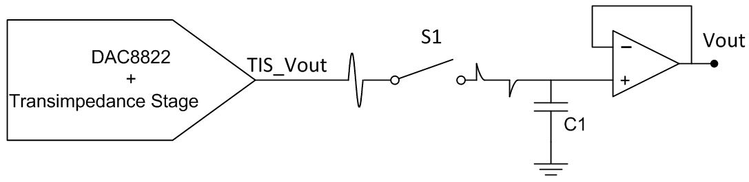
This thread has been locked.
If you have a related question, please click the "Ask a related question" button in the top right corner. The newly created question will be automatically linked to this question.
Hello Asaka-san,
Ryuji Asaka said:Could you please let me know any idea for reducing the Midscale DAC glitch ?
A Sample and Hold circuit is another solution instead of the LPF. Since the DAC8822 outputs current, the S&H circuit should be ideally placed after the current to voltage conversion of the transimpedance stage.
Take a look at the circuit below.
The switch S1 is open during the glitch pulse, the previous DAC voltage level is maintained at Vout by the charge leftover at C1. After the glitch has settled, S1 closes and charges C1 with the new voltage.
This is just a diagram of the circuit. The actual implementation which includes the control circuitry for detecting the glitch and controlling S1 is much more complex. The S&H circuit is not recommended unless absolutely necessary because it will increase the number of components and the footprint of the design.
To summarize:
The glitch specification refers to the energy of the impulse (area below the curve). The energy must be conserved according to the law of conservation of energy, therefore, the glitch energy has to be dissipated somewhere in the signal path. By adding a low pass filter, the energy is conserved and is spread out across a wider time frame, which reduces the amplitude. The only other alternative is to break the signal path. The S&H circuit accomplishes this but in doing so, lower energy glitches are appear when the switch opens and closes.
I would suggest using the LPF and finding the compromise between an acceptable glitch amplitude and an acceptable settling time. Keep in mind that the worst glitch will typically occur at this midscale “major carry” transition (0x7FFF to 0x8000). “Major carry” refers to a code step in which all the switches inside the DAC change position; the switching action is what injects this energy into the signal path.
In order to make an accurate recommendation, I need to ask you a few questions.
Ryuji Asaka said:<Question 2>
Is glitch polarity(over shoot or undershoot) decided below transition ?
Please let me know each polarity of below.-7FFFh to 8000h
-8000h to 7FFFH
Refer to Figures 14, 15, 30 & 31 in the DAC8822 datasheet. The increasing codes will always have an undershoot. The decreasing codes will depend on VDD. At 5V they will be overshoots. At 2.7V they will be smaller magnitude undershoots.
Ryuji Asaka said:<Question 3>
Could you please let me know the distribution data of glich peak voltage ?
In our customer, VDD is 3.3V and Vref is +/-8.192V bipolar operation.
Are you referring to the distribution across units? This is typically a Gaussian distribution. The typical value represents the mean of this distribution.
Asaka-san,
Take your time. I will wait for the answer.
Ryuji Asaka said:Can I use the Figure 14 as typical value of peak voltage of MIDSCALE DAC GLITCH (about 43mV)?
Yes. You can use this as a typical value for your peak voltage, but keep in mind that this only applies for an unloaded DAC8822. The shape of the curve will change depending on your load.
Hello Asaka-san,
Unfortunately there is no distribution data for glitch.
Are you interested in decreasing the glitch peak voltage only? Or managing the glitch energy?
Asaka-san,
I understand. However, I just wanted to let you know that if your customer is interested in a private discussion, we can also accommodate that.
Let me know if you need anything else.
Best Regards,