This thread has been locked.

If you have a related question, please click the "Ask a related question" button in the top right corner. The newly created question will be automatically linked to this question.

Writing to ADS8201 registers

Other Parts Discussed in Thread: ADS8201

I'm having trouble writing to any registers on the ADS8201.  When I try to read from the registers on the chip, I get the expected power-on default values.  However, if I write to a register and then read it back, I'm still getting the power-on default value.

Here's an example:

0576.ads8201_sequence.tiff

The commands in the above sequence are:

0xA4AA - software reset

0x6000 - read reg 0x8 (returns 0x02, the expected register value after reset, though data sheet suggests SDO should output all ones on the operation following a reset)

0xA000 - write 0x00 to reg 0x8

0x6000 - read reg 0x8 (expected 0x00, still returns 0x02)

0x9005 - write 0x05 to reg 0x4

0x5000 - read reg 0x4 (returns 0x00, expected 0x05)

0x9403 - write 0x03 to reg 0x5

0x9800 - write 0x00 to reg 0x6

0xA005 - write 0x05 to reg 0x8

0x6000 - read reg 0x8 (still returns 0x02, expected 0x05)

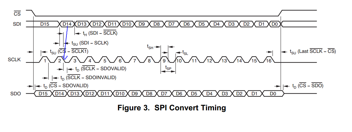
The SPI mode is set to 0, SCK frequency is 1.3MHz.

4810.ads8201_spi.tiff

I've looked at all the signals on an oscilloscope and they all look clean.  I've also tried multiple ADS8201 parts, but they've all shown the same behavior.

Any help would be appreciated.  I must be missing something subtle.

  • Nathen, 

    It seems to me that you have configured the SPI master of the system to latch data in the positive slope of the clock signal where the ADS8201 expects the SPI data to be on the negative slope.

    I suggest re-configuring the SPI master in this system to have match the ADS device.

    Regards,
    /TA

  • Thanks.  That was the piece I was missing.

    Confusingly, TIers in other threads have suggested that SPI mode 0 (clock idles low, sample on rising edge) is correct.  Also, the chip outputs data on the falling edge, suggesting it should be sampled on the rising edge, but I guess sampling on the falling edge should still work if the microcontroller's hold time is reasonably low--it just doesn't match the standard SPI timing diagrams.  Anyway, I bit-banged something that seems to work (can read and write registers), and now I'll try to get it working with the SPI peripheral.

  • Maybe I am just slow, but to help others avoid several hours of hair pulling "fun", the important thing to note in the timing diagram is that the SDI and SDO are not on the same clock edge. This means that you must use a different SPI mode depending on if you are reading or writing. When you read, use SPI mode 0. When you write, using SPI mode 1. I am guessing this was a design error discovered after the fact, as there is no mention of any of this in the datasheet. If this was by design, it would have been clearly emphasized in the datasheet. I have never encountered this in my years of talking to SPI devices.