This thread has been locked.

If you have a related question, please click the "Ask a related question" button in the top right corner. The newly created question will be automatically linked to this question.

ADS8319 trouble with busy indicator in daisy chaine mode

Other Parts Discussed in Thread: ADS8319, ADS1278

Hello,

My config use 2 ADS8319, I met 2 issues type, not all parts are concerned, only some time to time (about 20%):

1) busy indicator in first position in daisy chaine is not at the correct place related to clk (it appear at low level of clk between falling edge and rising edge clk - any other clock are present in the design) (see D3 on next picture
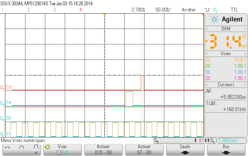
info:

D1 = Clk, D3 = SDO (1st part)

2) the number of bit transfered from the first part to the second one is greater than the 16 bits expected (1 more bit) so all conversions are  improperly read (see next picture - Busy indicator of 1st part seems to be read as data by the 2nd part !!)

Other info:

D1 = Clk, D5 = SDO of first part, D4 = SDO of 2nd Part

Fclk = 35MHz Fsmpl = 100KSmpl/S,

Schematic is based on  datasheet application (ADS8319 P 18)

Those issues, when append, are present on all frames all time (not a glitch or aleas).

by exchanging part issue is (are) solved.

Do you have some advice or track to understand that and correct it.

Thank you in advance

Alain

  • Alain,

    Thank you for your post on the ADS8319.

    You have mentioned a couple of oscilloscope captures in your message, but the attachement is missing.

    Could you please post these captures and the relevant sections of schematics of your board to help us solve this issue you are facing?

    Thanks.

    Regards,

    Sandeep

  • Sandeep,

    Thank you, I have upgraded my post.

    Regards,

    Alain

  • Alain,

    Thank you.

    Your first question is now clear and is not a cause of concern. As mentioned in page 13 of the datasheet, the ADS8319 does has an internal (interface independent) clock that is used to run the conversions. The busy indicator can go high between 1.1-1.4us after the rise edge of CNV based on this internal clock and does not derive its timing from the SCLK of the SPI interface.

    The second question looks like a timing issue. Could you please elaborate on “by exchanging part issue is solved” – are you replacing one/both of the devices or are you interchanging the order of devices on the daisy chain?

    Regards,

    Sandeep

  • Sandeep,

    Thank you for you answer,

    I fact first point is not yet solved. I agree with you about delay time between start of conversion and rising edge of busy indicator. However Busy in,dicator is build to be read from SDI at falling edge of clk. You could observe it fall down before it can be read! so busy indicator function is unavailable in this case.

    For 2nd issue, I have replace, each time where this problem append, the second part in daisy chaine (the signal from the first part was ok and does not need to be replaced ).

    Regards,

    Alain

  • Alain,

    I sat down with one of the designers of the ADS8319 and went over this in detail.

    There is a window of uncertainty to when the busy signal would be driven high and this number can show part to part variation. With a free running SCLK as you have used in your implementation, there is a possibility of missing the BUSY signal with some parts.

    The intended method to use the “Daisy Chain Mode with Busy Indicator” mode, as shown in Fig. 55 of the datasheet, is to use the SDO of the closest ADC as a interrupt (IRQ) to the host. Only after the IRQ is received, should the host start driving the required number of SCLK edges to the device to read the conversion results.

    Also in order to correctly configure the devices to generate the Busy Indicator at the end of conversion, it is necessary that SCLK is high at the rising edge of CONVST (it might be a bit tricky to ensure this condition with a free running SCLK). CONVST must continue to remain high from the start of the conversion until all of the data bits are read. Hope you have taken care of these conditions in your design.

    I would recommend that you move your implementation from a continuously running interface clock to a bursty SCLK generated when the devices indicate that data is available.

    Regards,

    Sandeep

  • Sandeep,

    Thank you.

    For your last answer part, yes design had taken care and met required conditions specified in datasheet in all termes you mention.

    For the first answer part, yes my design is equal fig 55 execpt SDO does not connected to IRQ but to another serial converter (ADS1278). FPGA look Inside the frame busy indicator of last ADS8319 to start unserialiser. As you understand SCLK provide also SCLK for ADS1278 wich can not be stop (burst SCLK is not possible here).

    Well, know I am not sure if it could be usable using busy indicator as "interrupt" FPGA using here, treate all available signal on clock edge => what does mean interrupt if busy indicator in not present at any front of any clock! And when / where have to start deserialiser (which next falling edge is the MSB).

    Another point, what about my 2nd issue.

    Regards,

    Alain

  • Alain,

    The 2nd issue is most likely a marginality in the capture timing. The fact that it varies from part to part also points to this. You should try running the design at a much slower clock speed to confirm. With the marginality removed, it should be easy to pick the location of the bits to be captured.

    The ADS1278 in the daisy chain introduces a new set of questions. The max SCLK speed of the ADS1278 is 27MHz, but your first post mentions that your design runs at 35MHz.

    The ADS1278, as far as I can tell, will not correctly handle the busy bit generated by the ADS8319, but you could deal with in you FPGA code.

    If you are not using the busy indicator to interrupt the host, why configure in “Daisy Chain Mode With Busy Indicator” mode at all? Would “Daisy Chain Mode Without Busy Indicator” not be a better option?

    Thanks.

    Regards,

    Sandeep


  • Sandeep,

    I am sorry but I am not sure to understand you answer about the 2nd issue: If I count number of edge from clk face to SO DATA, I find One more bit at the 2nd part SO again the right number at the SO of first part. I had supposed in normaly situation Busy indicator was removed when transmit from the first part to the second. And in this situation some timing issue shift baddly busy indicator. !! 

    About max frequency of ASD1278, you have right initialy we work bellow 27MHz and we rised to 35MHz without detect any problem  at 35MHz (I do not see if some characteristics are downgrade). 

    For you proposal working without busy indicator, I a not sure if it is possible or not. If I read well data sheet, conversion time is between 600nS and 1400nS. In this case how located the first bit (SCLK is continue)?

    Thanks.

    Regards,

    Alain

  • Alain,

    A question I forgot to ask in my last post – is you setup ADS8139>ADS8139>ADS1278>FPGA or is it ADS1278>ADS8139>ADS8139>FPGA? I am curious as you mentioned “SDO does not connected to IRQ but to another serial converter” but also that the “FPGA look Inside the frame busy indicator of last ADS8319 to start unserialiser”.

    Either way, it would be really tricky to build a robust solution with all three parts daisy-chained to a single host running with a single free running SCLK.

    The idea behind the busy indicator on the ADS8139 was to enable the host to generate SCLK to gather data only after the data is ready. We have no control on when the ADS8319 generates the busy (which is based on its internal oscillator) and therefore some device will fail to meet the timing requirements. This is the behaviour you are observing.

    I am not aware of the pin/area constraints on your FPGA, but the cleanest solution would be to daisy chain the two ADS8319s to a SPI master on the FPGA supplying a bursty SCLK; and have the ADS1278 controlled by a second master running a continuous clock. And keep each clock within the particular device’s rated max. frequency limit.

    Regards,

    Sandeep

  • Hi Sandeep and Alain,

    here jumping on the loop as I've been involved through a parallel disty channel.

    Alain : are you ok with answers Sandeep gave so far?

    Sandeep : just add any further comments if you think it make sense.

    Thanks in advance for kind feedback about, best regards to all

    Sergio

  • Hi Sergio,

    Right know, no solution! Issues are little bit complicated.

    I am trying to understand well issues and what solution to give.

    Thank you.

    Alain

  • Sandeep,

    Just some more points: our setup is ADS8139>ADS8139>ADS1278>FPGA.

    Solution as you suggest using separate SCLK and SDO is not very easy, because this part of design is first fully isolated   and secondary design already in production phase. So heavy modifications are not easy.

    Perhaps another question, you proposed to use bursty SCLK mode, but how this mode could be solve the 2 initiates issues. 1) if busy indicator desappeared after 20nS without any raison. 2) length bits at the SDO of 2nd part is one more bit?

    The better solution should be to not use busy indicator (the both issues should not be any more concerned) however in our design I don't know how to proceed. Knowing that datasheet include busy indicator solution! 

    Why parts whith this fault was not detected and excluded from TI production (if it is parts the issue!)?

    Regards,

    Alain

  • Alain,

    I am guessing that the isolation is between the ADCs and FPGA (ADS8139>ADS8139>ADS1278>Isolation>FPGA) and that the FPGA is on the secondary design that is in production.

    We might be able to design some glue logic on the isolated ADC part to workaround this issue, but I really need more details to be able to help.

    -        How many I/Os do we have across the isolation and with what directions?

    -        What throughput and resolution requirements are you trying to meet for each analog input for your system? Is it not possible to meet these with a single class of ADCs?

    -        Is there a real need to drive the ADS1278 beyond the rated operating frequency, or is it being run faster just because is sits on the same daisy chain as the two ADS8139s.

    This last item is actually a big no-no. We cannot guarantee performance of a device beyond its rated operating conditions and do not recommend that you use it in this mode.

    Could you please share a system block diagram/schematics for this subsystem to help understand the constraints better?

    Regards,

    Sandeep

  • HI Sandeep,

    Right know that true I did not focus on accuracy of ADS1278, The main aim of this  is not absolute value but detected small variations (delta V in short periode of time). So we probably could return to 32MHZ (just datasheet specify 32.768MHZ not 27MHZ!) We are actualy relativly close.

    I join simple diagram to explain part of design (several board can be connected (FPGA is little bit full).

    Other I/O isolated are present but used for other I/O and DAC output.3527.synopt Current ADC.pdf

    Regards,

    Alain