This thread has been locked.

If you have a related question, please click the "Ask a related question" button in the top right corner. The newly created question will be automatically linked to this question.

ADC 5282 EVM Data Alignment Problem

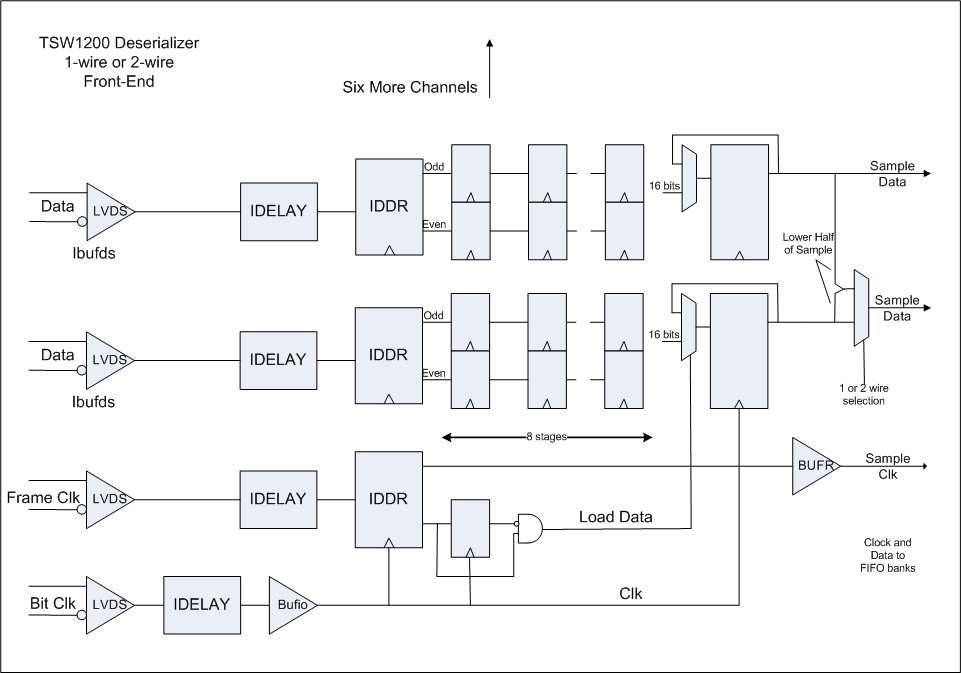
I am using the ADC 5282 evaluation module to capture data.  Currently I'm just trying to develop the code for it.  I'm using verilog and I've connected it to a terASIC DE4 FPGA board which uses a Stratix IV with on chip termination for LVDS.

Here are the test modes and data out:

Deskew: 0x555 (LSB First) or 0xAAA (MSB first)
Sync: 0x2F4 (LSB First) or 0xDOB (MSB first)

I delayed the Frame clock by 1 bit clock cycle and get the same Deskew values but differen Sync values.
Sync: 0xF42 (LSB First) or 0xOBD (MSB first)

I know the proper values are 0xFC0 or 0x03F.  I've added my SystemVerilog DDR and S2P blocks below.  I assume I am making a common mistake.  I also assume 0xAAA or 0x555 is the correct Deskew values.  I'm not sure where the problem is.  It looks like I have at least two bit flips.  

always @ (posedge ddr_clk or negedge reset) begin
	if (!reset) begin
		d_n		<= 1'b0;
		d_p		<= 1'b0;
	end else begin
		d_p		<=	ddr_in;
		d_n		<=	relatch;
	end
end

always @ (negedge ddr_clk or negedge reset) begin
	if (!reset) begin
		relatch		<= 1'b0;
	end else begin
		relatch		<=	ddr_in;
	end
end

always @ (posedge bit_clk or negedge reset) begin
	if (!reset) begin
		d0		<=	1'b0;
		d1		<=	1'b0;
		d2		<=	1'b0;
		d3		<=	1'b0;
		d4		<=	1'b0;
		d5		<=	1'b0;
		d6		<=	1'b0;
		d7		<=	1'b0;
		d8		<=	1'b0;
		d9		<=	1'b0;
		d10	<=	1'b0;
		d11	<=	1'b0;
	end else begin
		d1		<=	d3;
		d3		<=	d5;
		d5		<=	d7;
		d7		<=	d9;
		d9		<=	d11;
		d11	<=	d_n;
		
		d0		<=	d2;
		d2		<=	d4;
		d4		<=	d6;
		d6		<=	d8;
		d8		<=	d10;
		d10	<=	d_p;
	end
end

always @ (posedge frame_clk or negedge reset) begin
	if (!reset) begin
		word	<=	12'b0;
	end else begin
		word	<=	{d11, d10, d9, d8, d7, d6, d5, d4, d3, d2, d1, d0};
	end
end
endmodule 

  • Hi,

    what sample rate are you running that code at?  It looks like you are creating your input DDR block out of logic rather than using an input DDR cell made for the purpose.  I have not coded this up for Stratix before, but in Xilinx and Lattice there are special cells (such as an IDDR in Xilinx and several such cells such as IDDRX2D1 in Lattice) that are built to handle the speed.  I don't know if your Altera tools will be smart enough to replace your code with an input DDR cell, but if not then you will likely run into speed limitation problems.

    After that i see you are building a chain of shift-register style flip flops.   That's fine.  Then you use the rising edge of frame clock to 'catch' a sample's-worth of data bits.  Is the Frame Clock brought in on a similar clock input as the bit clock so as to match delays between the bit clock and Frame Clock?

    In my Xilinx and Lattice designs i have not tried to use Frame Clock in this manner.  Frame Clock has the same data setup adn hold timing around the bit clock as any other data line has.  I prefer to think of the Frame Clock as an extra data channel that happens to have a known data pattern in it such that i can use it to 'see' where the sample boundary is on the other data lines.  That is, i use the bit clock to latch the frame clock like any other data input and then process the data and frame clock in logic clocked off the bit clock.  Or if using a IDDR cell that breaks the data stream down into not just even/odd at bit clock rate but rather down into even1/odd1/even2/odd2 at half that rate - then i clock my deserialization at that rate.

    Please see the attached sketch on how i did it.

    I never could get frame clock timing of the rising edge constrained well enough to the other clock so as to use the rising edge of the frame clock as the deserialization clock directly.

    But for the actual code you posted - i dont see a logic flaw yet.

    Regards,

    Richard P.

  • Thank you for replying and sharing your experience.

    I am running the device at 10 MHz.  The goal is to be able to run it at 65 MHz without error.  We probably will never run it at this speed, but it would be nice to know the system is robust enough to handle it.

    I gave the LVDS RX IP core one more chance and it actually worked.  I don't know what my problem was in the past that prevented it from working.  Perhaps I wasn't familiar enough with what I should be seeing.  

    So, now the LVDS RX block outputs a 96 bit word and a frame clock.  I then divide the 96 bits into the 8 channels and send them to a sync manager.  The sync manager deals with aligning the value to a known test value (0xFC0) to the frame clock.  I am able to re-align 0xE07 to the correct value 0xFC0 in real time.  The problem I run into is when I switch from test patterns to actual values, I get garbage (see attached).  

    Between the vertical blue and red lines is roughly 5 micro seconds, half of a cycle of a triangle wave.  So now I'm trying to figure out why it isn't correct.  The Aqua Line is the digitized analog signal and the logic analyzer software is displaying the value as an analog value.  The Red line is the serialized bit stream.  

    Do you have any suggestions?

    Code:

    always @ (posedge frame_clk or negedge reset) begin
    	if (!reset) begin
    		word_temp			<=	24'b0;
    		skew_count		<=	4'b0;
    	end else begin
    		word_temp[23:12]	<=	word_in;
    		word_temp[11:0]	<=	word_temp[23:12];
    		case (skew_count)
    			0:		word_out	<=	word_temp[11:0];
    			1:		word_out	<=	word_temp[12:1];
    			2:		word_out	<=	word_temp[13:2];
    			3:		word_out	<=	word_temp[14:3];
    			4:		word_out	<=	word_temp[15:4];
    			5:		word_out	<=	word_temp[16:5];
    			6:		word_out	<=	word_temp[17:6];
    			7:		word_out	<=	word_temp[18:7];
    			8:		word_out	<=	word_temp[19:8];
    			9:		word_out	<=	word_temp[20:9];
    			10:	word_out	<=	word_temp[21:10];
    			11:	word_out	<=	word_temp[22:11];
    			default:	word_out	<=	word_temp[11:0];
    		endcase
    		
    		//1111_1100_0000
    		if (sync_enable) begin	//Look for the Sync Word
    			case (word_temp)
    				24'b1111_1100_0000_1111_1100_0000:	//Zero Skew
    					skew_count	<=	4'd0;
    				24'b111_1100_0000_1111_1100_0000_1:	//1 Skew
    					skew_count	<=	4'd1;
    				24'b11_1100_0000_1111_1100_0000_11:	//2 Skew
    					skew_count	<=	4'd2;
    				24'b1_1100_0000_1111_1100_0000_111:	//3 Skew
    					skew_count	<=	4'd3;
    				24'b1100_0000_1111_1100_0000_1111:	//4 Skew
    					skew_count	<=	4'd4;
    				24'b100_0000_1111_1100_0000_1111_1:	//5 Skew
    					skew_count	<=	4'd5;
    				24'b00_0000_1111_1100_0000_1111_11:	//6 Skew
    					skew_count	<=	4'd6;
    				24'b0_0000_1111_1100_0000_1111_110:	//7 Skew
    					skew_count	<=	4'd7;
    				24'b0000_1111_1100_0000_1111_1100:	//8 Skew
    					skew_count	<=	4'd8;
    				24'b000_1111_1100_0000_1111_1100_0:	//9 Skew
    					skew_count	<=	4'd9;
    				24'b00_1111_1100_0000_1111_1100_00:	//10 Skew
    					skew_count	<=	4'd10;
    				24'b0_1111_1100_0000_1111_1100_000:	//11 Skew
    					skew_count	<=	4'd11;
    				default:
    					skew_count	<=	4'd0;
    			endcase //word_temp
    		end else //Sync_Enable
    			skew_count	<=	skew_count;
    	end // Else CLK
    end //Always