A related question is a question created from another question. When the related question is created, it will be automatically linked to the original question.
If you have a related question, please click the "Ask a related question" button in the top right corner. The newly created question will be automatically linked to this question.
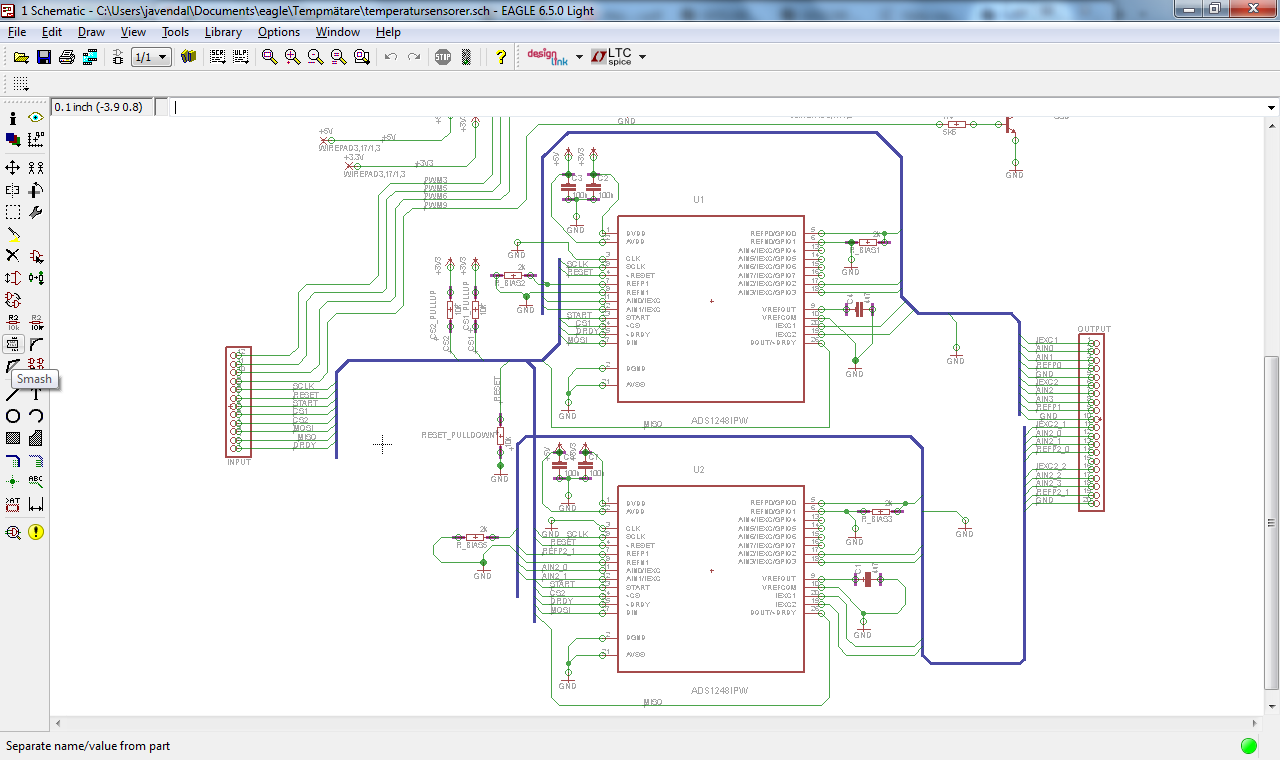
I'm new to the SPI-protocols. I have trouble to initiate communication between my Arduio UNO and the ADS1248 chip. Could you please have a look at my setup and check that everything is in order.
I don't see anything in your schematic that would prevent communication. Before communication can take place, the device must be powered, the RESET pin must be high, and the START pin must be high. There is also a wait period after power up before attempting to communicate. This time is given in the datasheet.
The SPI is Mode 1. SCLK should dwell low, with data changing on the rising edge of SCLK and stable (read) at the falling edge. Data is transferred in bytes, but make sure CS is low throughout the entire communication transaction. For example reading data by command (RDATA) is a 4 byte transaction. The first byte is the command followed by 3 bytes of data. CS must remain low throughout the entire time and must not toggle within the byte frames.
Can you send scope/logic analyzer shots of the communication?
On my PCB manufactured according to previously attached schematics I'm not able to pulldown the voltage on the CS-pin to more than 4V when the ADS1248 is soldered to the PCB.
Does this imply that there is something broken in the chip?
It is not required to have pullups or pulldowns on the pins you mentioned, but having these resistors does allow the ADS1248 to power up in a known state while the controller is initializing. The ADS1248 will not function if the RESET pin is low, so the controller connection to this pin must be set to logic high. The START pin is like a power down pin, so for the ADS1248 to convert, or to read/write the registers, the ADS1248 needs to be powered up which means that this pin must be logic high.
As there are two ADS1248 devices on your board, you will need to use CS to communicate to these devices separately. Again, using the pullups will keep the devices from accidently driving the DOUT pins at the same time on power up. The primary pins to monitor with a scope are CS, SCLK, DIN and DOUT. You can look at DRDY to verify the device is functioning. If START (and RESET) is high then you can check to see if the part is active by monitoring the DRDY line with the scope to make sure the DRDY pulses at the default data rate (5sps or every 200ms).
If you cannot drive CS low, then you cannot communicate to the part. Do you see the issue with both ADS1248 devices? First you might recheck the layout to make sure that the footprint matches correctly for the ADS1248. The CS pin is a CMOS input pin with some ESD protection circuitry. If the ESD structure is damaged, then you might see an issue. This could have happened if the Absolute Maximum Ratings were exceeded. One way where the Absolute Maximums could be exceeded is by initially powering your digital with 3.3V while attempting to control the ADS1248 with 5V. This would force the ESD diodes into conduction. Long term excessive current will damage the ESD cell. So it is possible that the device was damaged if this condition occurred.
Thank you so much for your help. Indeed you've pinpointed my source of error to my faulty parts. I'll put on new converters and try to monitor the pins you suggested.
I've put on new ADS1248-chips and now the communication works. I retrieve data with the "recieve data once" command and my only problem is that I don't know how to utilize the DRDY-signal. Reading from the datasheet I don't need to wait for a DRDY_low to send the recieve data once (and recieve result).
Do I only need to wait for DRDY_low if I use the recieve data continously-command?
I'm glad to hear that you are making progress. The DRDY transitions from high to low to signal the last conversion result is ready to read. The best method for continuously reading the conversion results is to use an interrupt driven system that is activated by a high to low transition on the DRDY signal. You can also poll this pin to see if it is low, and then you can read out the results.
The default operating mode for the ADS1248 is RDATAC (read data continuously) and what that means is each time the conversion period completes the data is automatically posted to the output register. This means you don't need to send the RDATA (read data) command, but rather just send 24 SCLKs and capture the data. A couple of things to note with the first being that the results automatically post. This can be a problem if reading registers or even the data using the RDATA command if the update period occurs during the read. What will happen in this case is the data from the conversion results will replace the contents in the output shift register.
To prevent this from happening, one option is to make sure that your data is captured as soon as possible (by using an interrupt driven system) and then making sure that all of your data reading is done between conversion periods. The second option is to use the SDATAC (stop reading data continuously) which does not halt the conversion process but rather just the automatic posting of the results to the output register. While in this mode you can get the conversion results by using the RDATA command.
The second thing I wanted to mention is DRDY will go high following the first SCLK period after DRDY has transitioned low. This makes the use of polling of the pin a little easier to do. Also note that if no SCLKs are sent between conversion periods there will be a small pulse from low to high to low signaling that an update has occured.
Of course you can also use a combination of the two modes. What I normally do is register block reads, so I always place the ADS1248 in SDATAC mode before reading any register contents. Issuing the SDATAC command will take effect after the next DRDY, so I wait until DRDY goes low (using the interrupt method), read the results and then reading my registers. Once the register data is read, I return to RDATAC mode.
Is there a "startup"-time or "settling"-time for the RDATAC-command? Since I use two ADS1248 to retrieve my results I must keep track on which converter is sending DRDY and the only way to do that on a single DRDY-line is to stop one of the ADC's to send DRDY pulse. (Is DRDY-signals stopped when SDATAC-command is issued?)
Also I'm a bit concerned about the stability of my results. When I do readings I get anything within +-0.05 degrees C (I use 4-way measurement setup). Any thought on what this big fluctuation be due to?
I will add linear regulators on AVDD and AVSS do mitigate any noise from my PC PSU (switched). Is there any point in adding linear regulators also on digital supply voltage?
Could the fluctuation of the results be due to the dynamic range of the ADC? Since I use 4-way measurement setup I measure from about 100 ohm to 140 ohm. Would there be a point for me to use a 3-way measurement with compensation so that I measure 0 ohm to 40 ohm instead?
One additional question. If I use linear regulators do generate a +2.5 V and -2.5 V AVDD respectively AVSS is it wise to tie the AVSS to gnd with decoupling caps (100 nF)?
When issuing the RDATAC command, the command takes effect on the next completion of conversion (DRDY transitioning low). Keep in mind that with the START pin high, the ADS1248 is always converting (or continously converting). What the RDATAC mode does (which is the default startup mode) is to automatically place the conversion results in the output register so you can read the results directly without issuing a command (RDATA). In other words all you need to do in RDATAC mode is send 3 bytes worth of SCLK and retrieve the data sent out DOUT.
Sending the SDATAC command will stop the automatic posting of results to the output register. It does not stop conversions and the SDATAC command has no effect on DRDY. When the SDATAC command is issued, the current conversion taking place will be posted automatically and the next conversion following the SDATAC command will actually be in the SDATAC mode. So, the conversion that is taking place will be in RDATAC mode and when it finishes the next conversion will be in SDATAC mode.
Here is a concern I see and that is with tying the DRDY pins together. These are output pins that are always active (they do not tri-state with CS). You will have output driver contention when connecting these pins together. If you want to connect the pins to a single input then you must do so with logic devices (AND, NAND, OR, NOR, etc.). If you use an external clock source, you can keep both devices sychronized by having each ADS1248 using the same clock source. The START pin can be used to synchronize the conversions.
Regarding the supplies, the PSRR is pretty good so it is unlikely you will see much benefit by further regulating the DVDD supply. It is always a good idea to place decoupling caps near the device supply input pins. This would include AVSS to AGND when using bipolar supplies.
Noise is always a concern with respect to precision measurements. The difficulty is in finding the source of the noise. Without knowing the noise source it is difficult to know what to do to limit the noise. Also, when adding devices to compensate for the input range you can actually make the situation worse. Any added resistance in the input path will add noise and stability issues (drift) that can affect the total error of the measurement. I would stay with the 4-wire RTD as this should provide the best overall measurment if you follow the information in SBAA201 (http://www.ti.com/litv/pdf/sbaa201).
Ok. So could I just skip the DRDY-channel and tie Dout together and use the combined Dout/DRDY-function?
It seems to work for me to read and write register with this setup but when I retrieve data there seems to be some issue. I read in the datasheet that when CS is high the chip shouldn't react to any SPI-commands and also Dout has high impedance. I believe I should be able to put only one CS low and send RDATA command and retrieve result from selected chip without conflict with the other chip.
To use the combined function of DOUT/DRDY you must set the IDAC0 register bit 3 high. When using the DRDY only signal, the pin is always active (never goes into tri-state) whereas the DOUT/DRDY signal will tri-state when CS goes high. So unless CS is low, you will never recognize that DOUT/DRDY has transitioned low. If you use CS and poll the DOUT/DRDY pin, you should use a pull-up on this pin so the signal line is never in an undertermined state.
One other thing to note about DRDY. Whether you CS or not, any SCLK clock seen on the ADS1248 input will drive the DRDY pin high. The logic that drives the state of the pin is totally independent of the SPI bus. For the DOUT/DRDY pin, following the read of data you may have to send a NOP to force the DOUT/DRDY pin back high if you use a polling method.
After I do the reading with CS still low I send the NOP-command to toggle DOUT/DRDY high. After NOP-command I set CS high and chose another chip.
My question is: When I want to read from the first chip again do I need to send NOP-command again before reading? Or do the chip remember that I've already sent it and I can read the DOUT/DRDY output and start to read the data directly if signal is low?
The important thing is to capture the transition of DOUT/DRDY from high to low to indicate when the new data is available. If the DOUT/DRDY is already low and you just start clocking the data, you run the risk that new data is available while you are clocking SCLK. In that case, the output data register is updated and your data is corrupted because you read out the first bits of the last data, and the first bits of the next data.
Problems may depend on where in the conversion cycle you are on each device. I'm not sure how you have the DOUT/DRDY connected, but I'm assuming that you used logic to combine the two DOUT/DRDY pins together. It might be helpful if you posted a schematic or portion of the schematic to show what you've done.
One sequence could be to setup one device, setup the other device and wait for the data to be read out with a single read for each device once both DRDY lines were indicated. That could be the safest way of getting data as long as you could quickly setup both devices and quickly read the data before either device came up with another data. I would be concerned if there were problems with what you read on DOUT/DRDY for one device, if the other device that you were not reading completed a read and the DRDY returned low.
I do not use logic to combine the signal. I just tie them together and use a pull up on that line. I believe this should be ok since the DOUT/DRDY-signal enters a high impedance state when CS is high.
My thought is to:
1. Set CS low
2. Send RDATAC
3. send NOP to set DOUT/DRDY-signal high
4. Wait untill DOUT/DRDY turns low
5. Retrieve results
6. Send SDATAC
7. Set CS high
and then same procedure for the next chip.
This seems to work but my problem now is that the results I receive are corrupt.
Maybe 3 out of 5 retrieved results are reasonable whilst the other look something like 111111000000 or 1000. I am considering if this is due to noisy digital signal. Any thought on what this may derive from?
If it is a noisy digital line that corrupts the results it is strange that all my read- and write- register commands always works flawlessly.
Also this error does not occur when I increase the data rate to 80SPS (compared to my normal operation at 20SPS).
I'll try to look at the signals in an oscilloscope.
Looking at your method, it generally looks correct to me. I don't see any obvious problems with the way that you have it set up.
For the noise problem, I think it would be best to see a scope shot of the communications. If you have some sort of logic analyzer to check communications, that would help as well.
I'm not sure what kind problem you're having, but you might be able to test to see if it is noise if you change your DRDY MODE bit to 1. That would force the DOUT/DRDY high upon receiving 24 SCLKs. If there is noise then you would see the DOUT/DRDY go high most times when there is an error.
Another thing that you might try would be to add some capacitance from SCLK to GND to clean up this line. If you do have noise, the SCLK line would be the most sensitive.
I will say that I don't think it's noise. I find it unlikely that you would have any difference in readout performance between the 80 SPS to the 20 SPS, especially if the data were being clocked out at the same rate. I would suspect that there might be a coding or communication error that might cause this problem. Regardless, an oscilloscope shot or logic analyzer data would be a great help in debug.
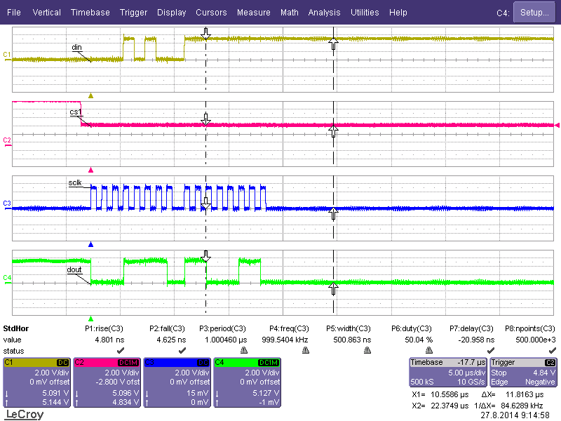
Here's a screen shoot of the communication. DIN and SCLK are measured close to the chip and CS and DOUT are measured close to the controller. The offset voltage shown on CS1 is incorrect. The signal indeed varies between 0V and 5V.
I send a RDATAC command followed by a NOP to pull DOUT high (I've set the DRDY MODE bit to 1).
So I believe I should have only 0 on DOUT when I send the RDATAC-command? Do I need to empty the register before I send the RDATAC-command?
Clearly I'm doing something wrong. What are you thought on how noisy these lines are?
Just to let you know, the plots look ok. I would not suspect noise to be corrupting any data. However, let me point out two things.
First, the default readout of the ADS1248 is with RDATAC. So when the device starts up, SCLKs will immediately start clocking out data on the output register.
Second, if you do issue an SDATAC, it doesn't clear the data from the output register. It simply stops updating there. So if you had issued an SDATAC to stop data, you'd still need to clock out the data to bring DRDY/DOUT high.
Going back to your plot, it looks ok depending on what you had asked the part to do.
If you had just started the part, the default would have started the device in RDATAC mode and the device would started giving data immediately when SCLKs were clocked in. In the case where you were expecting 0s to come out, you would have had to start with a bit of setup. First, you would have had to send an SDATAC command to stop the data from being updated on the output register, then you would need to wait for the next /DRDY to finish the next conversion. Then you would need to clock out the last conversion so nothing remains on the output register. After setting up the device this way, you could restart the RDATAC. Then issuing the command, DATA comes out after the RDATAC command and not during it.
If you're having problems with bad data, there are a few things I would try. First, get the scope shot of the bad data similar to what you have. However, if you only have 4 channels, then I would drop the /CS line (and assume that it's correct) and get the /DRDY line. It's a bit more important, and more people have problems with syncing the data retrieval with that line. That's where I'd start, especially when the data error is intermittent.
If the error always occurs, I'd look at the offset calibration register and the full-scale calibration register to make sure the values make sense. If they don't, I'd check to see if they are written to or if there was a calibration done to set them off.
As I wrote earlier I do not use the DRDY-line to check if conversion is ready. I've tied DOUT/DRDY together of my two chips and set the DRDY MODE bit to 1 for both devices.
In that case I guess it would be like this at startup:
The concern that I had was that in the datasheet, it says that the SDATAC takes effect after the next /DRDY. I wanted to make sure that the output register was completely cleared.
I never managed to get the converters to communicate correctly with the DOUT/DRDY signals combined. Instead I re-routed separate DRDY-signals for the two chips I'm using and readout the results with interrupts.
This now seems to work as (some of) the results seems reasonable. But I still have issues with the results. Actually the only trustworthy results I can measure is the AVDD and the DVDD voltages. Here I consistently measure 4.8V respectively 5.1V which is also what I measure with my multimeter. Everything else is just off.
E.g. I set IDAC current to be 1mA and I measure arout 0.88mA with my multimeter. R_ref voltage is 2.1V and I measure 1.8V with the chip. With the inboard temperature sensor I read a temperature of 42 degrees in the chip when I use it in room temperature. With 4-wire RTD measurments my readout varies +-5 degrees between result readouts.
Another question: the MSB in the result readout is the sign, right? Is 0 positive and 1 negative?
To you have any thought on what these problems might derive from? I have build everything in an old PSU from a PC. Do you think the PCU could cause these problems?
I'm glad you were able to get some usable data out.
Starting with the IDAC current, I would note that the initial error is only 6% max. I will say that you are further off from that value, but consider these things. First make sure that the IDAC output isn't forced high in voltage. There can be a reduction in current compliance when the output current is driven high in voltage above 4.3V (assuming AVDD=5V). Another thing to look for is other current leakage paths from the IDAC output. If there are ESD or TVS diodes on those pins, they may have a current leakage. Also consider the possible error of the meter that you are using.
However, I noticed that if you are using the 2k resistor through the IDAC as the reference and you are getting 2.1V, then your IDAC current is 1.05mA. Let me know if I've confused your explanation of what you are doing.
If you're using the internal temperature sensor, the note that it's not guaranteed. However, I've looked as some of the original characterization and final test data, and the error is about 2C for a single standard deviation. If your internal temperature sensor is reading 42C, that seems a bit high for room temperature.
For the data format, the ADS1248 uses a two's complement notation. In that respect, an MSB of 1 will indicate a negative number, but the remaining numbers still follow two's compliment. There's a discussion in the datasheet on page 35, including Table 17 explaining the output.
When it comes to the PSU, I assume that you are referring to using a power supply from an old PC. I've never tried it, but it is certainly possible that it might be noisy and it could throw off enough EMI to create problems. Any switched supply might cause problems with digital lines because of the instantaneous current needed in digital circuits. Generally some sort of LDO might smooth some of the noise, but I'd be very careful about the noise you might get from this setup.
I indeed use 5V AVDD and 0V AVSS. Even though my schematics says that I use 2k res. for reference I actually DO use 2k4. Something is funky here.
After some more measurements on my board I've noticed that the AVDD sinks to 4V when I turn the internal reference voltage on (VREFCON:01). Any thoughts on why this happens? Do I have to change the AD-converters? Are they broken?
When I measure VREF_out with the reference turned on I measure 2.045V respectively 2.048V from the two AD:s.
My first thought is that your power supply is having problems. I'm not sure what supply you are using, but if its a strong power supply, and the device is pulling down the AVDD with turning on the reference, I would have guessed that the device would get very warm. If it isn't a strong supply you might be pulling it down with a bad load regulation of the supply.
If the supply is poorly regulated, this might cause other problems, so make sure that this is operating properly.
The thing I would consider is that the reference is pretty close to what you would expect in normal operation. Also, you have been getting data out of it - although sometimes there is bad data (which could be caused by a problematic supply).
To eliminate this as a problem, I'd try running this board off of a different power supply which is well regulated and clean. I've often used the low voltage part of an E3631A to make measurements. This also gives a reading of the amount of current that the board takes. If you are having issues with the supply being pulled down, getting a current reading may help.
One thing I came to think about is how the internal reference should be routed in the ref. mux. As I previously wrote I measure 2.1V between REFP0 and REFN0. Maybe this voltage is the internal reference and not the IDAC over R_ref? I need internal reference to be on for IDAC but it shouldn't be connected to REF0 input pair, right? If this is the case this would also explain why my voltage drops when I turn on internal reference. I use a variable voltage regulator for my power supply and the output voltage is set by a voltage divider. My guess is that turning on the internal reference in the ADacs connects either VREFOUT or REFPX to the AVDD (somehos). From VREFOUT and REFPX there are two 2k4 resistances (one for each chip) connected to GND that alters the voltage divider.
The voltage regulator anyway doesn't get warm. The reason I use these regulators for the board is that I want to mitigate any power supply ripple that my switched PSU might generate.
I have tried to use an other power supply with well regulated and clean voltage but all my data read problems still remains (but maybe not the voltage drop). I'm really clueless on what might be the problem here.
When I do "normal measurements" I typically read results in one region when the DR is set to 5,10 or 20 SPS and then my reading s mystically change into another level when I use 40,80 or 160 SPS. I notice in table 7 on page 25 that input current changes also between these data rates. Could this give a clue to what is wrong?
Maybe if I give some more examples, numbers and explanations of my problems you might be able to point me in the right direction?
Sorry I missed your last post, I was out last Friday and didn't see this one.
I'm not sure if the voltage is part of the internal reference, but you can test that can't you? Change the value coming out of the IDAC and see if there's a corresponding change with the reference voltage.
If your measurements change with the data rate, there may be quite few reasons for it. If you continue to post descriptions and examples, I'll continue to try to help. Just try to be specific and detailed about the experiments you've tried and the results.
First, I think you need to find out why the AVDD is dropping to 4V when you change settings on the device. If you're having problems with load regulation, that could be leading to a lot of other problems in operation and measurement of the device. That's why I asked if you had used a different power supply.
At one point you had mentioned that maybe the internal reference had been routed to another reference. First, the internal reference needs to be on to make sure the IDAC is working. Second, the internal reference can be routed to the external through REFOUT, but it also can be routed to the REF0 input pair. This is described in the register definition for MUX1.
I assume that you're making a ratiometric measurement with the 2.4k resistor and the IEXC current. What is the resistance on your measurement channel? If it is ~1.5kOhms, then you might be losing compliance with the IEXC pin. Note that as that pin's voltage rises past AVDD-0.7V, you will start to lose current as the current source loses it's drive capability. You can use a multimeter the measure the voltage from IEXC1 or 2 to ground to check. How are you measuring the IDAC current? Do you measure the voltage across a known resistor? The resistor used for the reference is 2.4k when the IDAC is 1mA, what is it for the other currents that you are measuring? Or does it stay the same?
Are there any other connections to the analog header that might be drawing current?
Can you post a different schematic than the one you've posted? It's a bit hard to read your schematic. In yours, all of the analog connections and all of the digital connections connect to a bus, so I can't see where the real connections are. If you have to hand draw a simple set of analog connections, that would be helpful.
So indeed the voltage drop was the problem. I find this a bit odd sine the power supply is supposed to source 1.5 A at 5V. What is the approximate power consumption for the analog part? I find on page 2 in the data sheet that the maximum input current is 0.1A.
For the first time I'm now able to do measurements! Many thanks for your kind help.
I'm glad you were able to get data out after figuring out the power supply drop was causing problems. I was worried that AVDD would drop low enough that you might get intermittent resets caused by the supply dropping out.
The amount of current consumed by the device depends on the mode of operation, but is outlined on page 4 of the datasheet in the power supply section of the electrical characterisitcs. Consider that it's about 200uA for the digital current, 200uA for the analog current, and another 200 for the on-board reference. Those are approximations, but you are below 1mA for the total.
I would still be worried that there is another current path on the board that is consuming power. You might want to check it by putting the device in sleep mode and checking the current consumption.
My problem was that my current supplies (LM317) for the analog part was oscilliating. With recommended capacitances on the output the current supply is now stable and all is working well.
I've been using these chip for some time now and I must say that I'm really imprest by them. Reliable measurments and SPI communications works well.