This thread has been locked.

If you have a related question, please click the "Ask a related question" button in the top right corner. The newly created question will be automatically linked to this question.

ADC16DV160CILQ LVPECL input

Other Parts Discussed in Thread: ADC16DV160

Hi , all


Let me ask a question about ADC16DV160.


My customer is trying to connect a clock generator (Analog devices_AD9520-4) to ADC(TI_ADC16DV160).


The sentence “An LVPECL and/or LVDS driver can also drive the ADC16DV160. However the full dynamic performance of the

ADC16DV160 might not be achieved due to the high noise floor of the driving circuit itself especially in high IF

sampling applications.” is written ADC16DV160 datasheet P21.In the case of output of clock generator is LVPECL,

what impact does this have upon ADC16DV160 ?


And , my customer is trying to design following circuit diagram ,

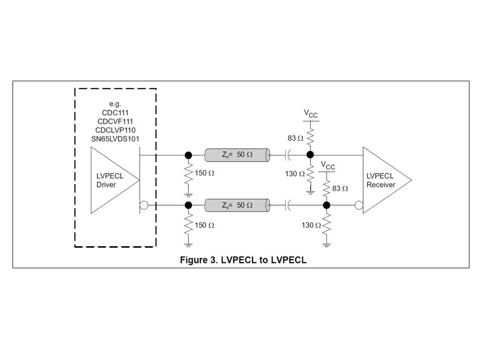
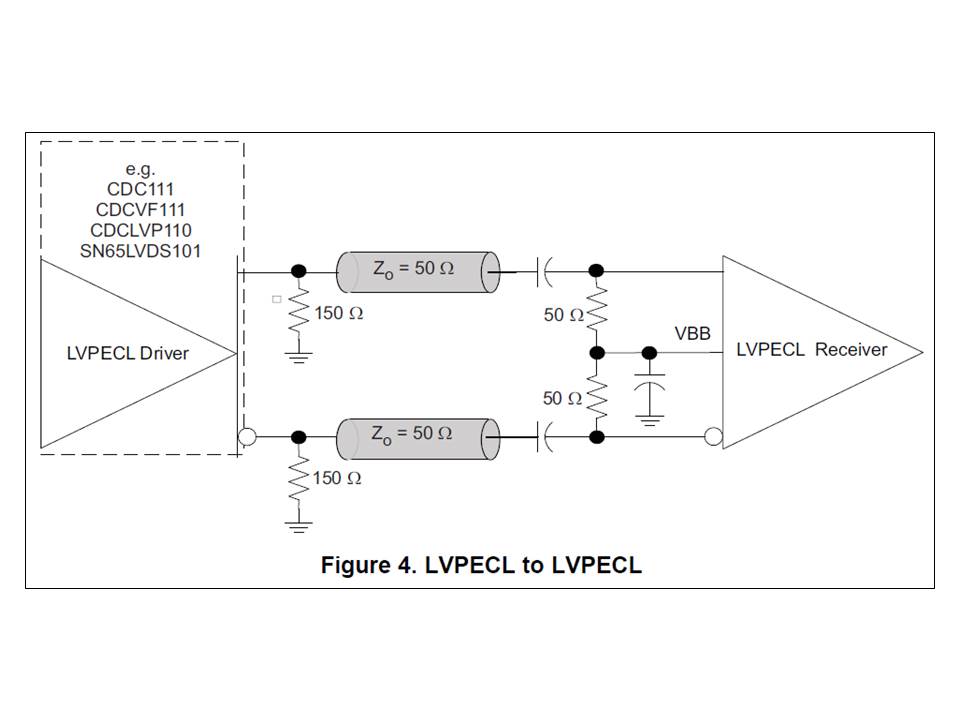
do you have a recommended circuit diagram to connect ADC16DV160 with LVPECL ?


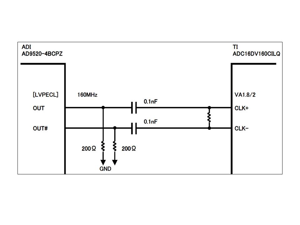
I think following circuit diagram is better, however ADC16DV160 has internal Va1.8/2 as datasheetP21 Figure32 so I think external Vbias is no need.


Best regards.

Taichi.

  • Taichi,

    The sentence in the datasheet that you refer to is related to the jitter in the clock signal path added by the ADC. This additive jitter is less when the edge rate of the clock signal is faster. LVPECL and LVDS will functionally work as clock signals, but LVDS in particular does not have a fast edge rate and therefore the jitter added by the ADC will be greater. This is most important when inputting very high frequencies into the ADC because jitter impacts the SNR performance more for high frequencies than for low frequencies.

    Any of the interfaces that you have attached are adequate, although there is no need to have an external DC bias on the ADC clock input because the ADC already has a weak internal DC bias.

    Regards, Josh